Created; 17/02/2016, Update; 04/07/2025 - 05/07/2025
This blogger page does not display all pictures in some web browsers, but at the present time current version of Edge seems to work better in May 2025. I have worked around the issue by uploading diagrams from my PC rather than loading them to this page from Google Drive. This Google Blogger also suffers from the common issue, bad formatting.
Partly worked through example - outdoor wireless environmental monitor.
Students either jump back and forth or overly work on a small detail. It is usual for a kindly elder to watch out for these and advise the student to put it down and move on to another aspect for a while, then come back to the problem later. It is also usual for an elder to advise a student to apply themselves. The student, elder and listening colleague roles are always useful and can be interchanged between engineers. The question is not known clearly until the answer is found. The answer is not clear until a period after the design is finished.
This example is worked through on a reasoned, prioritised basis as opposed to by a simple logical order. This priority-based approach is necessary to create a natural flow so that fellow engineers can start their work soon. The method requires judgment based on an understanding of critical path analysis. It also requires that the designer plan to carry out techniques in shorthand that he is well experienced in doing in longhand. That also means the draft design will jump about with the most difficult work done sooner and the reckoned to be easier work done later, and key component selection done as early as possible so the parts can be ordered soon to confirm what was expected of those parts, and that they can really be obtained.
 Stop and contemplate my design rather than leaping in and having second thoughts and undoing it all. But do get started, draw up and research some ideas and plan what you are going to do a little. A good tip that a management consultant gave in a place where plans went too far and too detailed was to; only plan as far as you can see.
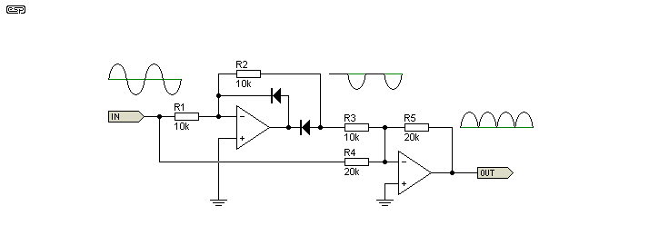
Peak detector circuits are not straightforward because there is a variable loop gain around the operational amplifier due to the diode switching, mitigated because that switching is soft drop in resistance as the forward current and voltage drop increases. There are extra components, C1, D2 and R4, to optimise the circuit stability to achieve accuracy and good bandwidth. The complication is that the loop gain changes because of the diode's variable impedance, and consequently, the circuit's bandwidth reduces as the input signal size reduces.
This example is worked through on a reasoned, prioritised basis as opposed to by a simple logical order. This priority-based approach is necessary to create a natural flow so that fellow engineers can start their work soon. The method requires judgment based on an understanding of critical path analysis. It also requires that the designer plan to carry out techniques in shorthand that he is well experienced in doing in longhand. That also means the draft design will jump about with the most difficult work done sooner and the reckoned to be easier work done later, and key component selection done as early as possible so the parts can be ordered soon to confirm what was expected of those parts, and that they can really be obtained.
- I use words like Reckoning to mean judgment and calculation based on experience and handed-down understanding.
- How to read this article - Imagine doing many of the different things in the sections below, but all at the same time. That is switching between aspects of the design so that you deal with or see an obstacle early.
- I used CADSTAR for circuit and PCB design on this page. This is a medium-performance CAD tool that is easy to start using, straightforward, but can be used to do good, sophisticated work. Unfortunately the CAD I had known, OrCAD-Cadence, had changed so much that I found the PCB tool Layout had been superseded by a much more manual or user macro-based tool, Allegro. So there is much more to getting started, and the training for the tool is very good, but there is no time or necessity for that now.
February 2016, with a Canon IXUS 60, contemplation, observing that the Crocuses by my front doorstep open in bright sunlight and close when the sun is dull.
.
Description - Outdoor wireless environmental monitor.
A
piece of test equipment is required to work outdoors and monitor
temperatures, vibration, air pressure, humidity and air speed. Battery
operation is sufficient, designed to conserve power somewhat, but not so
much that the design work would be long, highly refined and minimised.
This would not be a product for sale; therefore, some complications in
the electronics are okay if they save time, and some software work. A
similar design was used on a micro wind turbine project in 2009.

Peak detector (AL-0017-05B) Link to models for this function SiMetrix modelling CAD I have used is straightforward to use.
Peak detector circuits are not straightforward because there is a variable loop gain around the operational amplifier due to the diode switching, mitigated because that switching is soft drop in resistance as the forward current and voltage drop increases. There are extra components, C1, D2 and R4, to optimise the circuit stability to achieve accuracy and good bandwidth. The complication is that the loop gain changes because of the diode's variable impedance, and consequently, the circuit's bandwidth reduces as the input signal size reduces.
Ultimately, using good shortcuts gets you to the best solution in the given time. But the design is finished when the assumptions have been stated, returned to and are worked out fully. So keep notes such as;
- A To-Do list - things noted as I am carrying out design work and deleted when done. Significant items listed for later.
- A Mods list - recent changes only.
- And brief design Notes of key design points that are kept as part of a set of design drawings or software files.
---------- Outdoor wireless environmental monitor example -----------
ToDo list - Run notes on scrap paper or design page in your CAD drawing, keeping with the drawings in progress. The PCB is intentionally not completed for this Blog but is a preview of the almost final design and this is the circuit; AL-0016-04E. Print Screen gave me the best view but in any case this CAD uses solid colours rather than translucent colours so you can not see the tracks below.
 |
Work in progress AL-0016-04E. CADSTAR 16 Express - Free trial CAD tool. I have temporarily removed a the PCB module that has the board shape and the mounting holes in order to get further with the design. |
- Tidy layout. So that most tracks are on the bottom layer, and 0V plane is less fragmented.
- Configure track widths.
- Check the frequency and leakage characteristics of the capacitors.
- Recreate PCB shape with mounting holes.
- Check component sizes and clearances.
- Substitute the vibration sensor with a new type, such as PKGS-00LDP1-R.
- Carry out design calculations.
- Renumber and back-annotate.
- Amend the design calculations for the replaced op-amp now, TSV794.
Replace the dual op-amp with a fast quad, but with Rail to Rail i/o.
- Add an 0V plane underneath next to the connector so that i/o 1nF COG/NPO capacitors can be added.
- Fit PCB outline with 8 mounting holes.
The design process would continue while the parts were ordered. That is, I am switching between aspects of the job using the breaks to also consider my next step while I am working on the other aspects.
------------------------------------------------------------------
 |
| First sketch (AL 0016-01B) |
Component selection: Wireless - Xbee module;
 |
Thank you, Digi International, for the picture and
other support information. The gold circle is the aerial. The module's micro-controller is underneath as far from the RF aerial as practical. |
Digi Xbee wireless modules work well for this sort of application.
I have used 2.4GHz short-range (40M indoors or 120M in open space) Xbee radio modules. These modules have a serial port (TTL RS232), some digital I/O, SPI and some 10-bit analogue ports, and you can configure the ports to trade off for the desired combination of functions you require. These modules are similar to Wi-Fi but are used for lower-frequency signals.
Low power 2.4GHz, Zigbee protocol sounds like the best option, Xbee offering being a de facto standard and fairly international modules.
A pair or kit of these should be purchased, evaluated, and development should start now.
XB24-DMPIT-250 DigiMesh looks the most flexible, but is proprietary, though that would not matter. Mouser DigiKey £13 to £19
XB24CZ7PIT-004 ZigBee can relay data through intermediate nodes, and is called self-healing, is generic and slightly less flexible. DigiKey & Mouser £12 ea.
http://www.digi.com/pdf/ds_xbee_zigbee.pdf
XB24-API-001 XBee® 802.15.4 multipoint is less flexible, but looks adequate, and it is a generic protocol. This does not have the ability to relay data through intermediate nodes - so what, if they are near to each other, and anyway, consequently, the behaviour may be the most predictable and least RF workload. Farnell DigiKey RS £13 to £18 ea.
http://www.digi.com/pdf/ds_xbeemultipointmodules.pdf
Note: There are many other wireless network devices and protocols around. The board I have used as an example is well established with plenty of support. The prices are now very out of date.
Low power 2.4GHz, Zigbee protocol sounds like the best option, Xbee offering being a de facto standard and fairly international modules.
A pair or kit of these should be purchased, evaluated, and development should start now.
http://www.digi.com/pdf/ds_xbee_zigbee.pdf
XB24-API-001 XBee® 802.15.4 multipoint is less flexible, but looks adequate, and it is a generic protocol. This does not have the ability to relay data through intermediate nodes - so what, if they are near to each other, and anyway, consequently, the behaviour may be the most predictable and least RF workload. Farnell DigiKey RS £13 to £18 ea.
http://www.digi.com/pdf/ds_xbeemultipointmodules.pdf
Note: There are many other wireless network devices and protocols around. The board I have used as an example is well established with plenty of support. The prices are now very out of date.
Candidate new part number in 2025;
XB3-24Z8PT ~£30
XB3-24Z8PT-J ~£20
Concurrently;
The programmer should start studying the manual and developing the program; http://ftp1.digi.com/support/documentation/90002002.pdf This link does not work now. New link; https://www.digi.com/products/models/xb3-24z8pt
Notes from reading an XBee module's manual on what looks possible and useful;
- It appears that there is a supply voltage monitor A/D channel. This is useful because there was no spare A/D channel or capacity in this evaluation version of the CADSTAR tool I am using to add more circuitry. In any case, there is no intention to leave the module running more than a few days before recharging the batteries.
- Turn on input pull-up resistors as necessary to save adding resistors to the circuit.
- The internal temperature channel is not available with the general-purpose modules. But it is available with the PRO versions, I have read.
- Because the board is only for testing, it can be patched if necessary. It will not be resold.
These things need to be added to the to-do list and then checked.
All the components could be susceptible to the radio fields from the XBee module. So, ensure that power rails and input output have high-frequency capacitor decoupling. R.C filter and that voltage level be set mid common mode voltage range to avoid any diode rectification of picked up emissions.
- Motorola air pressure sensor - these are now made by NXP.
MP3H6115A pressure sensor has several pins marked do not connect (this is not the same as no internal connection - that I usually connect to 0V). Vs = 3V3, <8mA, o/p 47pF 51K.
This sensor should be ordered now. Wires and decoupling are attached when it arrives and evaluated for susceptibility to RF from the XBee module when moved near that module. A simple test that was little more than to see if the output changed when the unit was brought realistically near to the RF source and the pressure changed a bit.
- PT100 temperature sensors on 4-wire cable + instrumentation amplifier. These will need good screening and/or filtering because the cabling would act like an aerial.
- See: Electronics- Temperature measurement (resistor networks) - The temperature measurement circuit design is on another page.
Strategy for quick but confident design;
The Wireless part: The easiest way to use these modules is to configure them to communicate openly with each other as they find others nearby, but you can then use security to limit access as you get familiar with the modules.
Electromagnetic compatibility and good general filtering; Bandwidth limit, use digital filtering and for the XBee module, located on two rows of pins with 100nF and 1nF capacitors on power and analogue signals next to the pins. In retrospect, these additional filter capacitors are probably not required.
Write down your reasoning for expecting the unit to meet electromagnetic, susceptibility, radiated and conducted emissions and any tests carried out such as operate a mobile phone, a brush motor, or a radio does not detect interference very near the PCB. This is your evidence of having taken care and is called a technical construction file. A complaint is only likely too arise if you were to go into volume production with the unit untested, I am advised.
- Overly quick PCB design cost later,
- Some linear regulators oscillate at low power high frequency,
- Decoupling and 0V plane on the PCB do make a lot of difference,
- Resistor near op-amp output and capacitors at the inputs matters a lot. But putting a capacitor both ends of a track can be bad.
- Group signals and there return signal together, like a transmission line.
Motorola air pressure sensor - we can solder wires to pins and connect a Digital Volt Meter to the output, decouple the power and wire it to a power supply and then see that the output voltage is as expected and that it changes with pressure and how close to the XBee module it can be put without being adversely effected.
It turns out that this air pressure sensor works fine.
There is more on testing strategies similar to this evaluation on my website. I quickly tested and observed the correct output and an output change from approximately known inputs (atmospheric pressure, change and varying RF field). Since this project and other work in different industries, I have gained a better feel for RF sensitivity.
Metal canning for the electronics - Decided to risk not fitting any canning, but surface mount all the components under the motherboard and the Xbee module on top. In any case, we could probably retrofit canning if the idea does not work out, it is not going to be the smart unit for sale ever anyway.
The analogue to digital converter inputs have series resistors and capacitors for each analogue input of the XBee module.

AL 0016-01c The circuit above was created with CADSTAR 16.0 Express, limited-capacity free version of the tool. The PCB should come out under 60 mm^2.
This circuit is an earlier version that was used for the first design review. A price for PCB for say 3 or more should be obtained soon, and all the details required clarified so that a decision to continue or not can be made promptly.

- The first draft temperature measurement circuit is at the top left corner of the diagram above. More details at Electronics- Temperature measurement (resistor networks). After checking the data sheet for the instrument amplifier, it turns out that this particular circuit would not work.
The temperature circuit is changed to three channels instead of two, see AL-0016-02c right. The 8 input filter capacitors on the left are placed best, but an acceptable compromise is to use just 2 input filter capacitors. But in mitigation, the mux switch has some ESD-protected built in.
 |
| AL-0016-02C First part placement shows us PCB area I used the automatic placement tool although it will not generate a placement anything like how the PCB will end up like. I had created a larger PCB area to start so that I have plenty of space to work in. |
Vibration sensor - There is an analogue solution, but a better Digital solution could be developed instead, but in this case, that will likely take more time.
- The digital solution relies on already having some developed routines, plus a chosen microcontroller start-up code. But then it would be straightforward. We do not have these things, though.
- Here is a preview of some ideas that I may develop later, but I have some other work to do first.
- Use a simple two-diode voltage doubler full-wave rectifier with a forward bias resistor to a negative supply to do the rectification. Duplicating the rectifier but with no input to provide some temperature compensation.
- Electronics - Peak detector circuits and models.
- Electronics - Peak to Peak detector circuits and models.
- The simple half-wave rectifier at the top of this page should be sufficient.
Also, do some more work on the temperature sensor; now we can see how things are fitting together.
----------------------------------------------------------------------
The enclosure;
 |
| Revised enclosure proposal (AL-0016-02b) |
Having listed and decided on sensors, see below the enclosure shown above and deciding which functions to provide can be set or set aside for now.
--------------------------------------------------------------------------------------------------
Coming back to the temperature function again;Review modelling to determine the approximate accuracy, then revise the circuit and consider the new design.
Temperature measurement function software workload.
Look at the circuit settling time and optimise for accuracy. There is an optimum fast, and the circuit will be susceptible to moderate frequency noise; too slow, and the circuit will be susceptible to low frequency noise such as thermal drift.
Look at the circuit settling time and optimise for accuracy. There is an optimum fast, and the circuit will be susceptible to moderate frequency noise; too slow, and the circuit will be susceptible to low frequency noise such as thermal drift.
- As before, see Electronics- Temperature measurement (resistor networks).
The XBee module.
All unused pins can be left unconnected - some have pull-up resistors (check this).
Microprocessor used is; MC9S08QE32 (Motorola) now NXP These were leading edge products in there time, that means that the design process was then longer but on the other hand the part was lead in being low noise, wide temperature range and is now very cost effective, simple, highly refined structure and are well established now. The Cosmic C compiler produces very robust code that you can not put a razor blade between the expectation, the output when audited with PC Lint and what the part does. The on-chip one-wire emulator runs the code you compiled, not special debug code, so when it was developed 20 years ago was a very special feature of Motorola products and now is very well established.
#RESET - Demo board uses an RC. This aspect of the microcontroller's data sheet is not clear. You find that with Motorola, good English writing, but it does not quite tell you precisely. But I know from using other parts that it most likely does need a reset signal to be input.
Chopper stabilisation of the temperature measurement function and this novel peak to peak detector shown were not considered;
The plan is to fit 1nF filter capacitors to the connector pins, but not show them on the circuit because there is no capacity within this limited version of the CAD for doing that. (AL-0016-03b).
The PCB, I have started to group functions together and to optimise there placement and routing. Meanwhile, this method helps me see and review all design aspects, including RF field susceptibility.
Microprocessor used is; MC9S08QE32 (Motorola) now NXP These were leading edge products in there time, that means that the design process was then longer but on the other hand the part was lead in being low noise, wide temperature range and is now very cost effective, simple, highly refined structure and are well established now. The Cosmic C compiler produces very robust code that you can not put a razor blade between the expectation, the output when audited with PC Lint and what the part does. The on-chip one-wire emulator runs the code you compiled, not special debug code, so when it was developed 20 years ago was a very special feature of Motorola products and now is very well established.
#RESET - Demo board uses an RC. This aspect of the microcontroller's data sheet is not clear. You find that with Motorola, good English writing, but it does not quite tell you precisely. But I know from using other parts that it most likely does need a reset signal to be input.
There are many historical perspectives like this one on Motorola on my website.
Chopper stabilisation of the temperature measurement function and this novel peak to peak detector shown were not considered;
 |
| AL-0016-03D The chopper stabilised temperature circuit is very good, would have required more software work over a wireless connection and was not considered. The novel peak detector does not work properly, was a risky novel idea that would not have been considered in a work environment in any case. |
The PCB draft does not work with this circuit now, the PCB footprint and a capacitor have been lost when the CADSTAR library got corrupted. The circuit is two big by about two parts.
----------------------------------------
 |
The PCB, I have started to group functions together and to optimise there placement and routing. Meanwhile, this method helps me see and review all design aspects, including RF field susceptibility.
A good strategy is to work on a circuit function, then autoeco (netlist) the function to the PCB and work on the placement and tracking of the function. Work between the circuit and PCB until you are fairly content with the function and the placement.
- Autoeco or netlist are the names of the click that passes the data from the circuit design to the PCB design sections of the tool.
- Back-annotation is the button that passes that from the PCB (such as re-annotation or track widths) to the circuit design section of the tool.
- Enhanced back-annotation need not be used, and setting track widths can be done in either tool, but back annotation or autoeco must be completed in the circuit designer or PCB designer promptly to keep both parts of the design synchronised.
---------------------------------------------------------------------------------
Component selection - other parts;
85.7 f/C per m^2/s or 0.84 pC/G, 770pF, >500MR. Looking at the graph, the frequency response falls below 15Hz, but there is a worthwhile frequency response at <5Hz.
The LIS2HH12TR MEMS module is a good solution, particularly because it measures acceleration in all 3 planes. It is connected by a simple two or three-wire SPI or I2C bus and costs about £1. However, the peak detector would need to be carried out in software, though the RF throughput need not be increased if that can be done locally.
TP36 temperature sensor with shutdown. - Removed the following first draft circuit in favour of a multichannel PT100 type temperature measurement.
TS9011SCX 3.3V reg. 17p 50 off
ZXCL330H5TA 3.3V reg with enable. 35p 10 off.
S-80922CNMC-G8ST2G-ND reset generator
ZXCL330H5TA 3.3V reg with enable. 35p 10 off.
- It is stable with a low ESR capacitor according to the data sheet. (This point was checked after the final PCB layout because a COG/NPO 1nF capacitor is routed close to the regulator.)
- It is a lower voltage drop regulator/reference.
- Not used based on the Microprocessor and Xbee module datasheet review.
Change the op-amp to:
TSV794 MCP652 MCP662 op-amp. Max Ib is 30pA at 85'C, offset 200uV or 700uV (max), 50MHz.
The components that would be on a long delivery, or cold be difficult to obtain, should be ordered by now.
Would need to be sampled every 20mS (assuming 5 time constants would be enough), but missing some data and sampling less frequently may be adequate We could abandon this function at this stage it is taking some time?
Kermet CL31A226MOCLNNC (better insulation resistance spec than others at 50MR ), 0805, X5R, 22uF 10V, +-20% (need to change the footprint and part on the PCB) is stocked in RS 891-9801 at 14p, 20 off.
The op-amp MCP662 can drive >+-40mA, but the curves only go as far as 10mA. The circuit was changed because of the flaw noted and transistor B-C junction will used as a diode but we must take care to select a transistor that will handle the maximum current which is op-amp output current of 150mA.
From; i=C.dv/dt, Then; dv/dt = i/C
dv/dt = 10mA/22uF (20mA typically)
1V/2.2mS
This is equivalent to turning 90' of a sine wave into a simple ramp. To find the maximum frequency limit, multiply by 4 (4 x 90' is 360')
About 100Hz = 1/(2.2mS x 4) - this looks rather a low frequency, but may be okay. Likely, the vibration sensor function would not be pursued at this point because
From above; but try 4u7F
dv/dt = 10mA/4u7F (20mA typically)
1V/470uS worst, 1V/230uS typically.
This increases the frequency to 500Hz - 1KHz. (This is a useful frequency range, but the circuit board - see below will need to be made stiffer by adding mounting holes.)
Holding the capacitors' time constant;
Time constant: 2.5mS = 470nF x 4K7 this is very short, and the A/D converter will need to be sampled every 250uS. This is not giving us an improvement over simply feeding the amplifier into an A/D channel.
Change; R3 and R8 to; 10R or 0R (as shown or none)
Change; C10 and C11 to 4u7F footprint 0805 (not shown in the section of the circuit above, but is at the A/D vibration inputs)
The minimum frequency of the circuit is: 5Hz = 22K * 1u5F * 2.pi (this calculation was carried out later and the capacitor changed in the final PCB, see below)
The ceramic capacitors have a temperature coefficient, and X5F is about 10% over the temperature range. I have not checked this, but selected a reasonable plastic capacitor. Temperature fluctuation would introduce thermal noise into the low-frequency small vibration sensing. The temperature coefficient of the capacitor should be checked.
The maximum frequency of the circuit due to feedback RC is; 75KHz = 2M2 * 1pF * 2.pi. (This capacitor may be changed.)
After doing some arthritic and coming back around again, the assumptions become clearer and they should now be stated or amended; therefore;
For the large signal case, the gain approaches 10100, which gives a bandwidth of 6MHz and accuracy to 1% up to 60KHz.
For the small signal case, the total diode drop is 2V500mV For 1mV input change (1G), the loop gain is 2000 = 2V/1mV, and the bandwidth is 30KHz = 60MHz/2000 This gives an accuracy of 1% up to 300Hz.
The performance of the Vibration sensor circuit is still not modelled because we do not know the size of the stabilisation capacitor. But we have a reasonable estimate.
The PCB is more developed, and some other aspects have come to more clear whilst working on the circuit. So the designer would go back to temperature and change the reference resistor to a single 105R 0.1%.
The components that would be on a long delivery, or cold be difficult to obtain, should be ordered by now.
--------------------------------------------------------------------------

THE CIRCUIT WITH THE MODIFIED TEMPERATURE MEASUREMENT PCB (-4E) HAS ONE PART TOO MANY TO WORK IN EXPRESS CADSTAR 16. I HAVE REMOVED ONE PART, THE BOARD OUTLINE AND MOUNTING HOLES PART IN ORDER TO PROCEED SEE FURTHER ABOVE.
 Vibration will only be sensed from one direction if this is considered in review, not adequate for safety monitoring, then a multi-axis MEMS sensor IC will need to be used, connected via a serial interface to the wireless module. Meanwhile, we can work on the arithmetic based on what we have so far, which should give us more clues on viability, whilst considering if there is a problem.


 The first circuit also requires a capacitor across R5 for circuit stability. The circuits could not both be smoothed and respond to sudden vibration they are required to unlike a precision peak detector circuit. Take care with the third and forth circuits they operate with the op-amps input fed current below the negative supply, this may be okay or it may cause the IC to malfuction. Datasheets are not always clear about what can happen although some do explain and it differs with IC type and technoligy used. Eitherway the IC should not come to harm if the current is modest.
The peak vibration detector below (mid right) now fits in the design, but the humidity sensor and the battery voltage sensing has been removed. The Temperature is now three channels rather than two channels, and a number of filter capacitors will need to be added that are not shown on the circuit. This design can be reviewed if the design is to be proceeded with, an enclosure needs to be selected, and the PCB shape finalised. To be tidied, the tracks optimised so that it will work on a two-layer PCB and the track thickness set. Finally, the design can be renumbered.

The vibration sensor function (lower middle) of this circuit is more complex, and gives less information
(there would be no spectrum analysis option). Still, the software is easier because less data
(there would be no spectrum analysis option). Still, the software is easier because less data
needs to be collected or processed. The circuit is a half-wave positive peak detector. (AL-0016-04E)
 Vibration will only be sensed from one direction if this is considered in review, not adequate for safety monitoring, then a multi-axis MEMS sensor IC will need to be used, connected via a serial interface to the wireless module. Meanwhile, we can work on the arithmetic based on what we have so far, which should give us more clues on viability, whilst considering if there is a problem.
 Circuit sheet (5) of Power supply plus capacitors that don't fit on the PCB but probably should be fitted. But from subsequent experience, these capacitors probably do not need to be fitted.
Circuit functions (4) that are not used. Humidity sensor and Battery voltage monitor.
The simple vibration fully wave rectifier is not accurate, but might be good enough for humidity shown and vibration sensing rather than the op-amp precision circuit shown. The rectifier requires a second pair of rectifiers to provide approximate temperature correction and offset cancelling. This is drawn as a discussion point rather than a final design. Duplicated connections need to be removed.
------------------------------------------------------------------
Traditional precision low and medium speed full wave rectifiers;
 |
| AL-0017-09A Halfwave peak detector |
The second circuit below with gain added may or may not fit it looks like there would be the same number of parts? These circuits were quickly discounted as they are too big or not suitable for this application. A peak detector was required for vibration sensing these circuits could be followed by a single peak detector as shown above which then becomes a full peak to peak detector.
Precision full wave rectifiers - for a humidity and vibration sensors.
- Two Traditional circuits have uniform input impedance negative and positive.
- The third and forth circuits ADI do not have symmetrical loading and must therefore be DC coupled.
They have a low unsymmetrical band width depending on the resistor values used.
The rectifier is not required for the humidity sensor because a humidity sensor modules can be purchased with analogue or serial data output. Subsequently to this blog being created there are microprocessor evaluation boards with nearly everything required on them and they are quite cheap.
-----------------------------------------------------------------------------------
2 Vibration sensor arithmetic.
2 Vibration sensor arithmetic.
The op-amp has been changed from MCP662 to TSV794 Quad 50MHz rail-rail I/O. Therefore bandwidth related figures should be reduced by 12%.
Holding capacitors;
- The series resistor for the A/D is 5K set by the A/D's input leakage. If we were to compromise the performance to get less than 1000, 1 the capacitor leakage needs to be > 5MR. What ceramic capacitor would that be?
Kermet XR4 package 1206 is at least 500MR.uf therefore, up to 100uF capacitor could be used (with no margin).
- Time constant; 500mS = 5K x 100uF.
Would need to be sampled every 20mS (assuming 5 time constants would be enough), but missing some data and sampling less frequently may be adequate We could abandon this function at this stage it is taking some time?
Kermet CL31A226MOCLNNC (better insulation resistance spec than others at 50MR ), 0805, X5R, 22uF 10V, +-20% (need to change the footprint and part on the PCB) is stocked in RS 891-9801 at 14p, 20 off.
This looks wrong - driving a 22uF at 1KHz, say, would require a lot of current? (This is not serious at this stage because a lower value capacitor with the same footprint can be fitted.)
Holding capacitors' effect on bandwidth;
From; i=C.dv/dt, Then; dv/dt = i/C
dv/dt = 10mA/22uF (20mA typically)
1V/2.2mS
This is equivalent to turning 90' of a sine wave into a simple ramp. To find the maximum frequency limit, multiply by 4 (4 x 90' is 360')
About 100Hz = 1/(2.2mS x 4) - this looks rather a low frequency, but may be okay. Likely, the vibration sensor function would not be pursued at this point because
From above; but try 4u7F
dv/dt = 10mA/4u7F (20mA typically)
1V/470uS worst, 1V/230uS typically.
This increases the frequency to 500Hz - 1KHz. (This is a useful frequency range, but the circuit board - see below will need to be made stiffer by adding mounting holes.)
Holding the capacitors' time constant;
- Check to see if the A/D sampling rate can be reduced, and if so, can the input series resistor be increased? Thereby increasing the time constant. Unfortunately, the microprocessor's datasheet gives no indication that this is possible.
- But the number of bits of accuracy can be sacrificed so that the input impedance can be increased.
We need another solution, and later on, another solution comes to mind. See the last circuit that is at the bottom of this page. The solution may be;
The hold capacitor loading resistors have been moved to high voltages so that a more constant and small bleed current discharges those capacitors.
The hold capacitor loading resistors have been moved to high voltages so that a more constant and small bleed current discharges those capacitors.
- We do not know what the firmware in the XBee module does, but we do know that Vref can be 1.8V to VCC, 12 bits and 2K series resistors are recommended for the microcontroller. But the module data sheets specifies; 4K7 and 10 bits accuracy.
- From the microcontroller data sheet, we can calculate that the A/D's input current that would cause a quarter-bit error is; 375nA=3V/(4000*2K).
- That is for our desired 3Vref.
- We could reduce that for 10 bits to <100nA, but we need to add on the transistor leakage current of 1nA to 100nA or more. So we use the figure, 375nA
- The resistor value that would draw this current from half the minimum supply, 1.5V, is R should be less than 4MR = 1.5/375nA.
- An allowance should be added for the transistor and feedback resistor current. This would be less than 1V/3M9, say, would add another 250nA (this will need to be considered again)
- The total capacitor bleed current is: 600uA = 375nA and 250nA. Rising towards 1uA at maximum voltage swing (a case that is less important and is discounted).
The new time constant is;
- For C = 4.7uF
- . dv/dt=600nA/4u7F
Gives; 127mV/Second
- Or 7.8mS/mV Corresponds to 7.8mS per 0.1G
Op-Amp stability
- Op-amp datasheet Graph 4-7 suggests that the op-amp is stable with 2R for capacitors of >=10nF, but the transistors provide resistance if it is needed anyway.
- We work on the peak to peak detector, but in the end find that the circuit can not be optimised to work over the signal amplitude range desired. At that stage, the circuit board has been ordered and the designer has continued to work on component optimisation. The circuit is eventually likely to accurately record large vibration signals, and this is useful.
Change; R3 and R8 to; 10R or 0R (as shown or none)
Change; C10 and C11 to 4u7F footprint 0805 (not shown in the section of the circuit above, but is at the A/D vibration inputs)
**** Put this hold-up time problem aside and check some other aspects. ***
Minimum frequency
The minimum frequency of the circuit is: 5Hz = 22K * 1u5F * 2.pi (this calculation was carried out later and the capacitor changed in the final PCB, see below)
The ceramic capacitors have a temperature coefficient, and X5F is about 10% over the temperature range. I have not checked this, but selected a reasonable plastic capacitor. Temperature fluctuation would introduce thermal noise into the low-frequency small vibration sensing. The temperature coefficient of the capacitor should be checked.
Circuit accuracy and bandwidth are due to the operational amplifier's gain bandwidth product, but without the holding capacitors
The maximum frequency of the circuit due to feedback RC is; 75KHz = 2M2 * 1pF * 2.pi. (This capacitor may be changed.)
After doing some arthritic and coming back around again, the assumptions become clearer and they should now be stated or amended; therefore;
- The loop gain is the ratio of the output to the input voltages.
- But in the large signal case, the gain is 10 (this has been changed from 100 compared to the circuit above)
- And the loop gain is still the ratio of the output to input voltages, but simply that in the small signal case.
The op-amp's Gain Bandwidth product is 60MHz
For the large signal case, the gain approaches 10
For the small signal case, the total diode drop is 2V
The performance of the Vibration sensor circuit is still not modelled because we do not know the size of the stabilisation capacitor. But we have a reasonable estimate.
It is reasonable to say that my workings are unclear at this stage. I have come back and improved the working and the circuit function. So now I have a good feel for the circuit. Peak detector circuits are slower than would seem at first, in any case, and this is because of the variable gain introduced by the diode(s) and the need for stability in all cases.
More consideration on saving components.
The PCB is more developed, and some other aspects have come to more clear whilst working on the circuit. So the designer would go back to temperature and change the reference resistor to a single 105R 0.1%.
Vibration sensor 1;
It would not work because it is only accurate at low current, low speed, when the voltage drop is small. But this should work for a humidity sensor.
Use a simple op-amp amplifier as in the first circuit, followed by a double diode voltage-doubling rectifier and a negative current bleed from a negative supply. Circuit AL-0016-4d, (4) not used functions above.
Fit a second double diode to partly correct the large errors introduced by the variable diode voltage drop. This will need a current source resistor bleeding current from an appropriate supply.
- Using https://www.omnicalculator.com/physics/shockley-diode to calculate with a 1uA load, the two diodes will drop 10 mV.
Vibration sensor 2;
Use the negative input of the op-amp so that the peak detector is combined with being a high-impedance input buffer stage.
Removing the input capacitor and moving the sensor to the negative input has been done in AL-0016-04d, and has turned out to be necessary.
Vibration sensor 3;
I have included this novel solution, which, although I can't see why, does not work properly, I would not have spent time on anyway when I was employed. 
- Changed two diodes for an NPN and a PNP transistor which combines switching the feedback path and to the conducting rectifier junction and peak detector rectifiers.
- This circuit did not work under all conditions and would not have been considered originally. I do work on the circuit more in another blog.
- Take care with modelling tools which I did not use when I was in work. They are great time-wasting tools that save a lot of soldering and junking of prototypes that would not have been done anyway in the past.

AL-0016-03D Revised Vibration sensor. The circuit uses low saturation voltage transistors and the component count is low compared to any conventional low voltage working peak to peak detector I can think of.
The circuit has about two too many components to be designed with CADSTAR Express 16, the free tool. There remain some undefined XBee module pins. These will need to be dealt with. This circuit uses too many components, so it is not going to be used. In any case, it is too adventurous to use. It turns out that after modelling, it does not work well without more complications. I have not explored such an adventurous design normally at work.
PNP:
BC857
- Base current maximum is; 100mA (pulse 200mA C or B) - Assume the same as the collector current.
- Saturation does not fall below 40mV typically.
DSS5220V Zetex
NPN:
BC847 similar spec. to its complement BC857
FSB619 Fairchild low saturation switching;
The transistor solution should give a nice progressive change over from feedback from each polarity. But it is difficult to fathom out (to use a word meaning analyse and understand), the circuit will work well, but may not have the bandwidth first envisaged.
Both transistors have a high collector leakage current of 100nA at 25'C. Worst case is not given, but a typical value of 1nA is given. It is likely that leakage current will double every 11 °C to 7'C (at higher temperatures). This is not good, but it is what we have to work with at the moment.
The PCB could now be ordered, and any remaining parts. But there is a risk.
In the meantime, FMMT717 and FMM617 Zetex should be obtained and evaluated.
This higher version of CADSTAR both helps and presses you to update all parts to the most current version. I have also copied one part from a CADSTAR 16 to 18 Library, which works easily. The parts were lost when a footprint library got corrupted - you need to run tidy in the library on each of the parts and footprint libraries with older versions of CADSTAR. Windows or Google Drive can lock a file, preventing programs working with that file may have been the issue?
PNP:
DSS5220V Zetex
- Curves give < 8mV at IC < 5mA
- Ib 300mA pulse 600mA.
FMMT717 Zetex
- <17mV sat. Curves give; <1mV at IC <1mA.
- Ib.max = 500mA
- No footprint change.
FSB619 Fairchild low saturation switching;
- <20mV, typically <10mV gain 10 at IC=10mA.
- Base current is not given, but the collector current is 2A max., and Ib is the graph that goes up to 200mA.
DSS30101L Zetex
- curves give <<20mV at IC<=10mA, gain 10.
FMM617 Zetex
- <14mV sat. Curves give; <2mV IC<10mA
- Ib.max = 500mA.
- No footprint change.
Both transistors have a high collector leakage current of 100nA at 25'C. Worst case is not given, but a typical value of 1nA is given. It is likely that leakage current will double every 11 °C to 7'C (at higher temperatures). This is not good, but it is what we have to work with at the moment.
The PCB could now be ordered, and any remaining parts. But there is a risk.
In the meantime, FMMT717 and FMM617 Zetex should be obtained and evaluated.
- The PNP transistor.
- Connect the base to 0V and wire a 3M9 between the collector and a 2V supply.
- Repeat the first step but with the collector resistor reduced to 100R.
- Connect a 47M between the emitter and a 2V supply.
- Connect a high-impedance voltmeter (DVM) between the C and E to measure the turn-on voltage.
- Repeat the test with the NPN transistor but with a -2V supply.
The conclusion will tell us whether the peak detector circuit will work or whether to omit components and directly connect the vibration circuit to an A/D channel. The alternative plan. The drawback would be the extra software work that I was trying to avoid.
Having done the component selection, here is some modelling using Spice tools. That I could have done with vero-board or PCB design, then modified and maybe the best way of doing this work.
But on returning to this function in a real case, I would not have developed the idea as far, but would have gone quickly to one of the conventional circuits, such as the circuit at the top of the page. The problem was also that I was trying to make this board using a limited-capacity free evaluation CAD tool. Although I have almost eliminated the need for this test following spice modelling of other variants of this circuit, I am not really sure if the model is over pessimistic about the design. I could go back and argue for simply splitting the design into two boards.
Having done the component selection, here is some modelling using Spice tools. That I could have done with vero-board or PCB design, then modified and maybe the best way of doing this work.
- Electronics - Positive and negative Peak detector circuits and models
- Electronics - Peak detector circuits and models
But on returning to this function in a real case, I would not have developed the idea as far, but would have gone quickly to one of the conventional circuits, such as the circuit at the top of the page. The problem was also that I was trying to make this board using a limited-capacity free evaluation CAD tool. Although I have almost eliminated the need for this test following spice modelling of other variants of this circuit, I am not really sure if the model is over pessimistic about the design. I could go back and argue for simply splitting the design into two boards.
-----------------------------------------------------------------------------------------------------------------
We can now check on other lower-priority things.
- The pressure sensor MP3H6115A warm-up time is 20mS, so it turns out to be almost trivial as far as power-saving circuitry usefulness.
This is nearly the final PCB ready to be made.
 AL-016-06G The final version for this blog has been moved to CADSTAR 18. The layout has been optimised to reduce 0V plane fragmentation; therefore, most tracks are underneath (red) and the 0V plane is on top (blue). The PR Editor routing tool is part of CADSTAR which does many of the same things but differently or better.

# Replaced LDO with MIC5239-3.3YS reverse protected type; therefore, remove the input protection diode.
# Added the missing 8 mounting hole PCB outline module and adjust the board outline.
# Corrected the design spreadsheet for the half peak detector now running from Third VC. Therefore change one resistor.
# Replaced parts now not in libraries with parts that are.
# Removed one decoupling capacitor, thereby reducing the number of parts to 49.
ToDos;
# Consider; S13R1D33-N4T1-U3 made by ABLIC is another suitable reverse protected regulator, cheaper possibly lower voltage drop but would have required another resistor.
# Consider; A reverse biased P-channel MOSFET could have formed a super low drop diode instead. Then more commonly available LDO regulator could have been used.
The design is now has 49 parts and the maximum 50 parts.
Vibration function;
- A similar PCB was finally ordered, some changes may be necessary, and in the main just requires components to be fitted between different pins that were originally designed for.
- Some components were not fitted. But the PCB outline did exist at the time.
- But the most inconvenient would be track cutting and thin wire additions.
Alternative Peak to Peak Detector Link to models for these circuits
The full circuit was not developed as much as this to have done so was not necessary. A micro-controller evaluation board could be found now with wireless, sensors, plus any extra sensors such as humidity and air pressure, placed on a veroboard motherboard for the evaluation board.
The full circuit was not developed as much as this to have done so was not necessary. A micro-controller evaluation board could be found now with wireless, sensors, plus any extra sensors such as humidity and air pressure, placed on a veroboard motherboard for the evaluation board.
-----------------------------------------------------------
Conclusion
This design example has been worked through, but with more options considered than were necessary in the real case. The points would be covered, or notes that have been dismissed or are unlikely to be worth the time working through. These can be considered for a revised design later. In this way, the risk of misunderstanding and design failure is very low. First time right is a traditional and good strategy I recommend, but I do not recommend over-engineering (which this has become for this blog), as doing such does not necessarily do what is necessary and expected.

These photographs were taken sitting on my front door step.

These photographs were taken sitting on my front door step.
Bright sunny day and the flowers have opened.
This sort of engineering by pragmatic judgement, calculation and freedom for incite to happen is what distinguished British Engineering. There is less and less of this style permitted, and in any case, it seems bosting about war and money-making are not impolite things that have always driven the UK. Risk of getting caught such as making a mistake often drives bad decision making. Cliché' US "suing culture", risk aversion, and cost cutting at all cost are now woven in to UK life, compared to my childhood in the 1960s and 70s.
Associated pages with more details.
- Electronics - Peak detector circuits and models
- Electronics - Peak to Peak detector circuits and models
- Vibration monitor: Digital solution
- Electronics - Simulation and Judgement LT Spice simulations.
Also see: http://www.andrew-lohmann.me.uk/engineer
Please comment below - Alternatively, comment generally on my electronics; Electronics Discussion
Back to; Electronics, Software & Robust Design
Please comment below - Alternatively, comment generally on my electronics; Electronics Discussion
Back to; Electronics, Software & Robust Design
No comments:
Post a Comment