Created; 19/03/2016, Changed 10/07/2025 - 09/07/2025
This project was created to evaluate circuit modelling tools. I never used these tools at work. This blog looks at some peak-to-peak detectors and evaluates a novel peak-to-peak detector using BJTs as diodes and for feedback path switching. But these circuits have not been made and tested using a soldering iron and an oscilloscope, so I don't know if they work. The BJT feedback switching circuit did not work over a range of conditions; by comparison, traditional circuits work but eventually I got a solution that works over a range of conditions although it is more noisy and less acurate.
Circuit modelling tools;
- SiMetrix This PSpice circuit modelling tool is the capacity-limited free version. It has excellent circuit entry, and adding spice models, you just click and drop them into the command window and then when you use the part first time, you may define the symbol and pins if it has not already worked that out for you.
- LTspice is not limited is a free, full-feature tool supported by ADI. It runs in Windows or a Windows simulator. Analog Devices has owned Linear Technology, the originator of the tool, for some years.
- Qspice, made by Qorvo, which I have not evaluated, is an upgrade of LTspice; both spice tools were developed by Mike Engelhardt.
- TI-Tina 9 This simulation tool is not capacity-limited, but it requires the use of at least one Texas Instruments part in your model (but this limitation may not apply now). Adding other models is a bit fiddly at first, but easy when you know how! Tina also offers a free, limited demo version.
- Cadence also offer modelling tools which seem to be muddled together with their Circuit and PCB design CAD. TI also offer this tool at no charge. But my view is that these tools should be kept separate, and I did not get far when I tried to evaluate this CAD. OrCAD capture is the best circuit design tool. If you ask your CADSTAR supplier they may give you a link to Cadence 17 free version.
The proposed peak-to-peak detector;

SiMetrix AL-0017-03F: There is a problem with the transistors in this model. The circuit requires the model to operate with some currents below the values that are specified in the datasheet. An alternative and better explanation is that the inter-electrode capacitances of the transistors couple a false feedback signal, and that results in the peak detection not occurring. The problem is apparent because the transistors' E-C voltage drop is higher than the 1mV expected.
The transistors have an inter-electrode capacitance of ~20pF, so in AC terms, all electrodes are connected together. That inter-electrode capacitance is small in comparison with the output load but large in comparison with the feedback. This is a different theory from the reasoning above. I had expected a smooth transition as the polarity changes, but this has not worked out. The circuit is limited by the number of components possible on SiMetrix, but this is not an issue in this case.

The diagram above is for: +-25mV 100Hz input x10.
- Red is the positive output; the peak has overshot and then settled properly later. Other wave forms (negative) cannot be seen at this scale.
- The Blue is the op-amp output.
- Grey-Green is the feedback.

The diagram above is for: +-25mV 2.5mS rise, fall and width input x10 as the previous graph.
I have zoomed in around where the output settles to about the expected value.
- Red is the positive output,
- Green is the negative output,
- Blue is the op-amp output,
- Grey-ish-Green is the feedback that should closely (within 1mV) follow one or other output when there is current flowing, but it does not.

2.5mV x 10 the model. different scaling
As before, the circuit is not working at this scale; we can now see that the transistors do not switch on and charge the capacitors, although there is adequate base current for this to happen. There are no adequate emitter or collector currents. I do not think the model operates correctly with some of the transistor currents below what is specified in the datasheet. Specifically operate below the collector, emitter currents and the specified hfe values given data sheet.
Some variations of this circuit's parameters caused SiMetrix to stop with an error. This may be a problem with the op-amp model? This is because a similar Time step error happened more often when using LT Spice IV.
-----------------------------------------------------------------
 Tina-TI AL-0018-03B is more or less the same circuit but for the use of a Texas Instruments operational amplifier. The model now works over a significant signal range but with an unacceptably low-value feedback resistor. This compromise is useful because we can see some more characteristics of this function, and it is all as expected. It turns out that the low value feedback impedance makes the circuit work well, and I have also tried a TLV365 op-amp in the same circuit, and a quick look it behaves the same, that is, there is no point in running all the tests again with a different amplifier.
 This model uses different transistors, but also, the Tina-TI is not limited in capacity, and both points are significant. These transistors operate at particularly low currents and have very flat gain characteristics, are low noise and low leakage current, but the saturation voltage is not good and is not specified at low currents.
These alternative transistors BC848 and BC858 have a specified gain at a lower current, but do not have a good and specified saturation voltage at low current by comparison. So there is limited value in putting them in the model. I wanted to see what happens; it could be enlightening, and it turned out that those small signal transistors work well, turn out to be a better solution.
 |
| Input +-2.5mV x10. |
The circuit is working well and works down to +-25uV x10. Unfortunately, the op-amp is not really suitable because of its high input current, although it is fine with this set of conditions - that is, with a low-value feedback resistor.
A possible explanation for why the circuit with transistors can not be modelled.
The model needs to be kept small for good speed and to fit within the maximum capacity of some tools; The first circuit on this page just fits.
The minimum feedback resistor current at normal gain would be 67nA, and this would correspond to an output voltage of about 33mV (for the 470K feedback resistor). At this current, the transistor would be turned on and current would probably be flowing between the emitter and the collector, but the model shows the emitter current coming from the base but not the collector. The model struggles probably because these figures are, in any case, beyond the given data.
The modelling does not advise me where limitations of the model have arisen, but it does behave a little differently with different transistors used. This is the most unusual circuit, which is partly why I have chosen to evaluate modelling tools using these circuits. I have refined the conventional design as well.
 |
Input +-25mV x10.
The circuit is working well but driving with square waves does not show function clearly because the transistors turn on or off so we do not see any linear transition region. But we do see the circuit work very well with a fast step input. |
 |
Input +-25mV x10 Zoomed in.
The small square wave is the input signal.
The large square wave is the feedback; it looks clean, which is expected of the smooth transition in polarity due to the nature anticipated of the transistor circuit. |
|
| Input +-25mV x10 Zoomed in. The small square wave is the input signal. |
The large square wave is the feedback. Looks clean, which is what I expected of the smooth transition in polarity due to the nature anticipated of the transistor circuit.
 |
Input +-2.5mV x10 Triangle wave input shows the linear region.
|
The big signal is the op-amp output. The triangle is the input. The two near-horizonal lines are the two rectified outputs.
 |
Input +-2.5mV x10, triangle wave zoomed into the top of the peak. |
We can see that the feedback resistors (which have too low a value) cause the discharge rate to increase when the transistor turns on, then we see a spike of voltage that will correspond to high charging current flowing into the hold capacitor.
 |
| Input +-25mV x10 triangle. |
A larger signal shows the characteristics described above more clearly.
 |
| Input +-25mV x10 triangle zoomed in. |
A larger signal shows the characteristics described above more clearly. The peak voltage stored is reduced as the transistor turns off and current is drained via the Emitter.
-------------------------------------------------
 |
AL-0017-04A SiMetrix model, but of a very similar circuit to the previous circuit, which uses low-current signal transistors.
|
This model, which uses a different PSspice for the transistors, does not work as well as the Tina-TI, but it does work better using FMMT617 and FMMT717 transistors instead of the ones shown. The data sheet shows a flat gain for 10uA to 10mA the transistors for the transistors shown. The model does not stretch beyond well beyond what is specified in the models, evidently?


Tina-TI models;
 |
| Input 2.5mS rise and fall top and bottom plateau +-50mV x10. |
- Blue - op-amp output.
- Red - Vibration+
- Green - Vibration-
- Dark Green - Feedback (Transistor emitters)
-------------------------------------------------------------------
Eliminate the variations and cut the circuit to the minimum, just the peak detector, so that we can see what is going on with minimal ambiguity. But because there is no amplification the circuit will operate faster.


Tina-TI models;
- AL-0018-04C, The first circuit has another op-amp, but operating in comparator mode. The first circuit's outputs are lower by 20mV to 100mV than expected, or can be about right with a large signal, but with different input frequencies.
- AL-0018-07A, The second circuit does not have a comparator. Its performance is the worst.
- AL-0018-08A, the third circuit is a simplification of the emitter's loading. The third circuit is best, that is, in the first and last cases, the resistor is required, and it needs to be a lower value than 10M.
The TLV7211 CMOS comparator would also do the job, but there is a benefit in using an op-amp; it will be slower with less noise, which is beneficial in this function block. Modern rail-rail op-amps work reasonably well as comparators; they are not slow coming out of saturation. The additional op-amp comparator has improved the circuit function; neither circuit works properly.
The 10M is connected to 0V or output, and the negative input changes the behaviour but does not make the circuit function as expected. These two circuits are the worst and tend to show an extra current flowing from the base to the emitter rather than the emitter tied to the collector. Also, switching the polarity of the transistor E and C made little difference, probably made the behaviour worse.
The last circuit uses a low-value resistor to 0V. It is therefore similar to the first circuit but shows that the bigger the loading, the better the circuit works. But other variants that I have posted one example, based on the first and circuit but using BC848 and BC858, works a lot better with the 10M unchanged, The model I have posted below with emitters loading resistor increased to 10K, works well although the output voltage is still a little in error.


AL-0018-10A and -10 B. This and a variant without the comparator is one of the best of a not-satisfactory solution - it works with large and small signals at the most demanding 1KHz and therefore lower frequencies. 5mV triangle wave.
-------------------------------------------------------------------

A conventional solution (left and below) models well and is a safe choice. These circuits have latitude for optimisation and improvement by comparison and are more modelable because components are all working within tightly defined parameters specified in the data sheets. Not all these models include the output buffer amplifier but are small therefore faster.
Left, AL-0017-08B peak-peak detector. SiMetrix
Below the rectified peak detector, the output is the highest of the positive or negative peaks.

Right, AL-0017-02B Full wave rectifier and peak detector. SiMetrix
Notice that the feedback capacitor is located similarly to the peak detector, but for the full-wave rectifier. I have therefore applied the lesson discovered and discussed elsewhere.

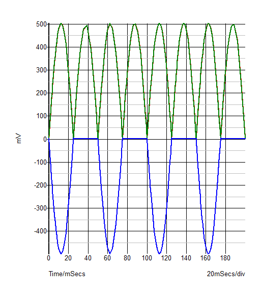
+-200mV 50Hz sine wave input.
- Blue - half-wave rectifier output.
- Green - Peak detector op-amp output. Pulses at the peaks.
- Red - peak detector.
----------------------------------------------------------------------------------------------------------------------------

AL-0017-06A Conventional precision signal full-wave rectifier.
Look at that first should help explain how it works - Output is: Halfwave output is x2 - x1, the input. C2 is 1pF and is for circuit stability, but if increased to 100nF would change the function to rectified and average.

- Left: Green is the output waveform, blue is the half-wave rectifier stage X4. (AL-0017-06A).
- Right, Green is the output waveform. Increased C2 to 100nF provides output averaging and is a typical variant of this circuit. (AL-0017-07A).
Conclusion;
The last diagram may not be useful in this application. The application was for various sensors on a machine, so peak vibration will probably be more useful in warning of failure or maintenance required. More likely, simply connecting the output of the motion sensor amplifier to an A/D input would give more detail because it is raw data, so that a noise spectrum analysis could be used, like an experienced mechanic may tell the fault in a machine by the sound it makes.
The last diagram may not be useful in this application. The application was for various sensors on a machine, so peak vibration will probably be more useful in warning of failure or maintenance required. More likely, simply connecting the output of the motion sensor amplifier to an A/D input would give more detail because it is raw data, so that a noise spectrum analysis could be used, like an experienced mechanic may tell the fault in a machine by the sound it makes.
It turns out that the novel BJT switching solution works but it took a lot of work and figuring to get to that point.
Thank you for the very instructive article.
ReplyDeleteI remember our technical specialists were working on the issue that took place in one of our data centers. That center must maintain the data room service. So we have implemented similar scheme.
Wow, its great post, its really important to understand how it works.
ReplyDeleteIts like my dissertation work, thank y.
security online
Possibly like your dissertation work I was satisfied with what I had developed over 35 years ago. I later find that it was the standard circuit anyway but with an extra diode that speeds it up a bit. Then to look again all this time later and refine the circuit even more because of the power of the simulation tools have allowing me the conveniently change things that I could not do conveniently do repeatedly with a soldering iron - so I stopped then.
DeleteWe never stop learning but I think I have learnt how to explain in words well since I was 19.
April 2018 - changes being made.
ReplyDelete