23/03/2016, Changed; 22/04/2018, 21-04-2018
The first circuit on the page Electronics - Robust Design methods (AL0016-01x) probably would do the desired job well. But if higher resolution and frequency were required the idea below could be developed. This circuit is more likely to be a starting point until a better solution comes to mind?
* In any case I've included this solution to emphasise the point (my website electronics first page) that a working solution on paper even if big is a good starting point.
There is a large data throughput to processor and/or send wirelessly. I have also included further refinements of the peak detector (discussed in other pages). The peak-detector condenses data throughput but also reduces the amount of data available.
****************************
The function block below is a mixture of circuit and block diagram and is a general purpose diagram for a range of non-analogue processing possibilities. They all look feasible in that the component count is reasonable. The choice is based on a requirement for a quick design and easy design but not necessarily costly.
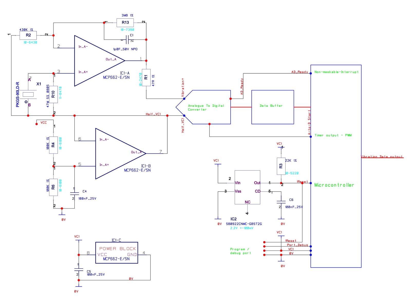 |
| General purpose mixed circuit and block diagram of a digital vibration monitor data collection and processing. CADSTAR Express 16 (AL-0019-01B) |
Possibilities are;
These solutions use more components than I had allowed myself. They also show other avenues and possibly are better solutions - I do not know for certain as I have not worked out a satisfactory explanation for what has been observed by modelling.

See; Electronics - Positive and negative Peak detector circuits and model
I have added an output buffer below to the models based on those in other blog pages.
--------------------------------------------------------------------------------

- Vibration sensor and amplifier. - All the individual analogue components shown are most likely unavoidable but we can check A/D converters that have integrated amplifiers?
- A/D converter - This could be one that is within the micro-controller.
- Data Buffer (1) - This could be programmable logic with a first-in-first memory buffer. The data then collected by the Xbee module in it's own time.
- Data Buffer (2) - Pseudo Direct Memory Access channel within a micro-controller transferring data from the A/D to RAM.
- Interrupt wire (1) - Without a buffer this would be used to interrupt the micro-controller so that data is collected on time. If the micro-controller is running with a very slow clock (to save power which is usually the most effective method) then that interrupt could be a non-maskable interrupt (NMI).
- NMI (2) - This sort of interrupt is different in different micro-controllers or may not be an option. NMI will interrupt another interrupt that is being handled that is a lower priority interrupt. Or it will interrupt itself and care must be taken to ensure that does not happen. It is a useful way to collect fast arriving data without lost instead of using DMA or a buffer.
- Reset controller - this is conveniently an IC. The micro-controller may generate it's own reset if one of the programme fault monitors is triggered. So in some cases a simple RC network is not suitable because this would conflict with the reset identification mechanism.
- Debug port the one shown is a Motorola one wire debugging port which has a small emulator and flash program memory programming support.
Analogue front end;
- It may be possible to connect the the vibration sensor to the input of an A/D converter possibilities;
- Audio types;
- CS5343/44 Cirrus Logic. These have remained the best delta-sigma converters available for at least few decades. This one is 3.3V to 5V and has a dual microphone 7 Meg ohm input. Cost £3 each Digi key.
- CS53L21 Cirrus Logic. low power 3.3V. Stereo with mic PGA. I2C or SPI bus plain and simple A/D. 4KHz sampling or faster. Direct input 20K, PGA 50K (not useful) Mouser £4 each.
- Industrial types (low frequency accuracy specified)
- CS5509 Cirrus Logic. External Ref. Up to 200 Sps. mouser £11.79
- CS5529 Cirrus logic. External ref. Digikey £8.30.
- CS5521/23 Cirrus logic. 4 Channel with PGA. 16 bit. specified up to 100 sps (faster may be possible with external clock? Instrument amplifier <300pA up to 40'C. Mouser £5.07/£5.67
- CS5525/26 No reference single channel, pre-amp, ext. ref. Spec to 200sps. digikey £8.05
- CS5530 No ref, single channel, pre-amp, up 3.8 Ksps. Mouser £4.49
- CS5532/34 No ref. pre-amp, 2/4 channel 3.8Ksps. Mouser £8.25/£8.61
- CS5500 Ref. x10 pre-amp, 2 channel. 2.4Ksps.
I abandoned this investigation at this stage to consider using more of a sledge hammer approach;
- Don't run the micro at low speed and therefore at low power.
- Therefore do not use Non-Maskable-Interrupt if something like that were available.
- Do use a micro-controller within internal A/D but in slower mode perhaps by selecting a high resolutions mode to reduce the sampling rate.
- Do not worry about making the interrupt handler short and fast (be careful though) but process the data a bit as it is collected.
- Include function calls for power saving routines that can be filled later.
- Also therefore use the microprocessor to do the temperature measurement and thereby pass resistance or temperature to the Xbee module instead of unprocessed numbers.
------------------- Peak detector solution further refinement ---------------
These solutions use more components than I had allowed myself. They also show other avenues and possibly are better solutions - I do not know for certain as I have not worked out a satisfactory explanation for what has been observed by modelling.

The
circuit above (AL-0020-02G) was created using LT spice IV. This circuit
does not use any LT spice model parts, other than generic passives and discrete;
Diodes Ltd, diode and bipolar junction transistor spice models all
work. The circuit is novel and demonstrates some useful features of
BJT's. An LT op-amp such as; LTC6088
works a little better in this circuit than the Texas Instruments op-amp
shown, which in some cases can fail to model and reports timing step
too small U3 but even so the TI model is much better than the MCP651
Microchip model. Both op-amps have a very similarly specification but
the LTC6088 is a lower bandwidth op-amp. LT Spice forum suggestion is
that where a non-LT model does not work then use the ideal model.
- Low saturation voltage (particular of these transistors);
- The capacitance between Base and Emitters provides a false feedback signal in the case of input signal <600mV pk-pk. The transistor's diode junctions in that case, of a small input signal at U3, never conducts and the outputs behave in an undesirable way as if the op-amp's output is just connected to the op-amp's -in, as in effect it is. C5 and C6 reduce this region of undesirable behaviour so that the circuit operates with input signals greater than >200mV pk-pk by in effect swamping much of the B-E capacitance. Anyway that is what I think is happening and the value of C5 and C6 is small compared to C2 and C3 so errors introduced by charge injected by those capacitors is small.
- Smooth transition rather than a hard switching characteristic brought about by the variable gain nature of BJTs is an added benefit compared to the conventional peak detector circuits similar to the circuit below. The region where the op-amp is operating open-loop is small by comparison with a conventional peak detector circuits.
- These transistors need to be physically tested to see if the circuit would work in reality for small signal case work. I am not sure that tools (LT Spice, Tina TI and SiMetrix) are modelling accurately.
- But
the model and data sheet do not define all parameters at the very
lowest currents and in any case the worst case data is not given but
just 25'C is given. This would have to be estimated but would make this
design marginal to use anyway.
See; Electronics - Positive and negative Peak detector circuits and model
------------------------------------- Improved conventional peak detector ---------------------------------------
I have added an output buffer below to the models based on those in other blog pages.


This circuit uses mostly LT spice model parts but the diodes use an NXP spice model. The circuit is widely used and this particular version has been refined some more using SiMetrix modelling tool and copied as a LT Spice which produces comparable results. The desired MCP651 Microchip op-amp model does not work in LT Spice IV but a Texas Instruments OPA365 and also the Linear Technology op-amps shown work fine. (AL-0020-01C)
- C4 has been relocated from between -in and out which allows the op-amp's output will change at the fastest rate when when the diodes are not conducting. In any case D1 resistance reduces progressively so there is not a sudden destabilising turn on. In any case tunnelling diode effect is not apparent or is handled well. Some parts of the output waveforms could be mistaken for tunnelling where the diode does not turn on until a higher voltage is reached than the normal forward voltage drop.
- R9 lowers the loop Q or to analyse it another way, prevents an additional delay in the loop that would have cased instability. These two design enhancements were carried as a consequence of using modelling tools to try things that might not have been convenient modification to a conventional PCB prototype. R9 is also shown in the manufactures data sheet as an application example.
- D2 limits the swing of the amplifier and prevents the output saturating. This aspect though may not be significant with modern op-amps and in this case the output can't swing far because of the low negative supply voltage.
- When designing a circuit and PCB a capacitor should be placed across D2 but not be fitted. It probably will be required.
The design is not trivial and there some artistic judgement involve see artistic design discussion at;
--------------------------------------------------------------------------------
A conventional solution is usually best.
Based on diagram on another page but with the output buffer added. These extra parts makes the model slow to simulate.
The circuit below demonstrates another point, that is; Do not include more function blocks in your simulation than you need. The amplifier stages around U2 and around U5 are trivial and without those circuit blocks this circuit, which is set to run a virtual 5 seconds, is resolved in about a minute and that is comparable to other tools. When U2 stage is added the circuit needs to run for longer on the PC for many minutes but with both U2 and U5 LT Spice was unable to resolve simulation using default setting in many hours. LT spice IV is fine in my opinion but I wanted to show an obvious point for myself, do not model more than is necessary. In this case those two amplifier stages can be modelled using pen, paper, and a calculator and in the simple buffer case by simply inspecting the op-amps data sheet and that will result in a properly understood and better job carried out more quickly.

In summary the conventional circuit
is the best. This circuit with one diode rather than two
diodes therefore relies on the op-amp coming out of saturation quickly -
the only clue that that mighty be fine is that a similar circuit is
shown in the data sheet but there is not a spec. point in the data-sheet
on how well the op-amp comes out of saturation.
In any case many low voltage op-amp's output's do come out of
saturation quickly. I have also modelled this with Tina-TI 9 and the
circuit also models fine. (AL-0020-05B).


This shows you how the outputs from simulation is presented (AL-0020-05A).
Feature of this circuit is;
The circuit is a little different and may operate with a lower supply voltage because the reification is only possessive so the op-amp supply voltage over-head is one diode voltage drop instead of two diode voltage drops 0.5 - 0.8V increase in voltage margin.
Feature of this circuit is;
The circuit is a little different and may operate with a lower supply voltage because the reification is only possessive so the op-amp supply voltage over-head is one diode voltage drop instead of two diode voltage drops 0.5 - 0.8V increase in voltage margin.
No comments:
Post a Comment