19-03-2016, Changed; 09/06/2025 - 10/06/2025
Modelling tools used;
- Tina-TI 9 or Tina, SiMetrix 9.20, and LT Spice 24, the LTspice support group, is good, the CAD is free, unrestricted and when first launched claimed to model faster and better than other tools. The other tools are the free versions. SiMetrix is the easiest, but LTspice is the most comprehensive. They produce similar results, but of course, they do not model circuit board parasitic components unless parts are added to represent the PCB parasitic components. Therefore, take care with the results and ensure you figure out what you want and what you expect before you start any modelling.
- By comparison, obviously, there are some points you can not test directly on a real circuit because the test probe will affect the circuit, such as the output of low-power, low-speed op-amps, and the high impedance part of fast circuits. An oscilloscope probe's capacitance is usually 10pF (x10) or 100pF (x1). Consequently, the model will let you see points in the circuit that you can not accurately probe, but take care to not become overconfident in the circuit reproducibility because the model results look good.
Tina-TI 9 conventional peak detector;
Tina-TI is now quite old, but it works well enough, though the graphical entry is poor and can leave warnings and errors that can not be resolved. You can download Tina-TI, and TI still offer models for it; you must use at least one Texas Instrument part in your design. Or use the Tina Simulator is also available; the free version has a design size limit.


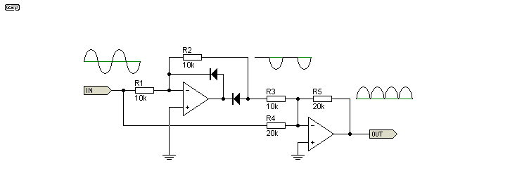
AL-0020-03H LTSpice & AL-0018-01C Tina-TI conventional peak detector circuit and a variant of a conventional circuit. The circuits have differences that may or may not improve them; the gain is 11.


AL-0020-03H LTSpice & AL-0018-01C Tina-TI conventional peak detector circuit and a variant of a conventional circuit. The circuits have differences that may or may not improve them; the gain is 11.
C1, C2, R2, and R5 feedback need to be set for the best speed and to just undershoot. R5 gives a linear softening rather than a diode curve softening of the switching point. A fast rail-to-rail I/O op-amp has been chosen, but a TSV494 would also be a good choice. D1 speeds up the switch by limiting the op-amps' output swing.
The LTspice circuit was drawn years ago on another PC I have changed the circuit, but the resistors were not brought in from the libraries; they had to be placed again, which means that their values are lost. Zig-Zag style resistors and other components were okay, though.
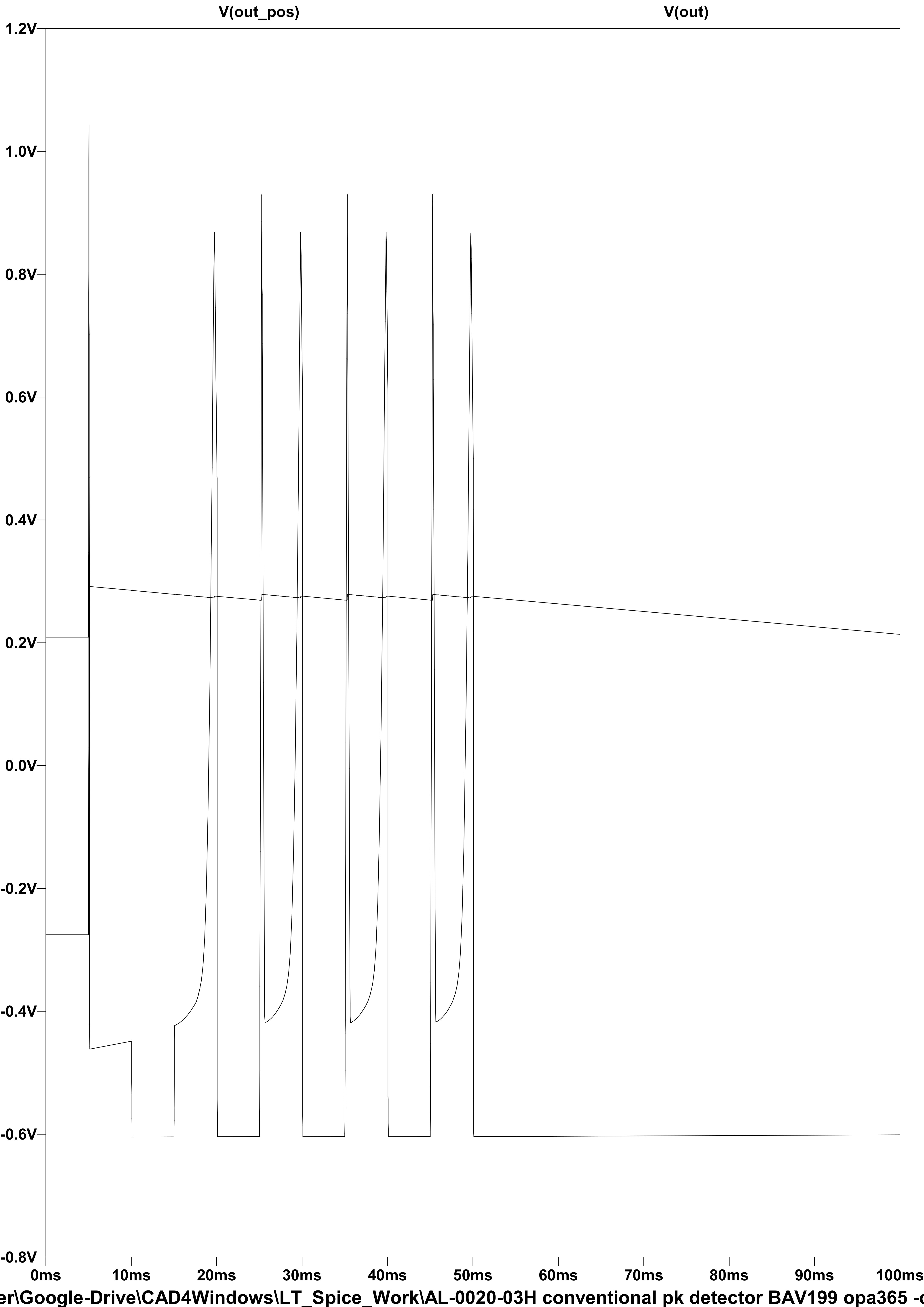

AL-0020-03H LTSpice & AL-0018-01C Tina-TI: The above circuits have a ±25mV peak-peak, 100Hz square wave input. Gain x11.
AL-0020-03H LTSpice C1=2p2 - the ripple is 10mV, overshoot 25mV [C1=220p also works]
AL-0018-01C Tina-TI - the ripple is 13mV~, overshoot 0mV~.

AL-0018-01C - Overshoot 0mV~, Ripple 20mV~.

AL-0018-01C - Undershoot 0mV~ and ripple 5mV~.

The ripple is ~9 mV, and no overshoot, Increasing C1 or changing that compensation does not improve the circuit.

You will need to reinstall some added parts if you move a design to another PC. In this case, copy and drop the BAV199 diode and OPA365 op-amp into SiMetrix. I changed the circuit to use this op-amp because it is a rail-rail i/o low Ib part.
- The op-amp gain bandwidth product is 50MHz, which at best could give a circuit accuracy of;
- At 1KHz, gain of 10; 50MHz/1KHz/10 = 5000:1
- The actual performance is a lot less good than this. I have found that a big margin is required with a peak detector.
- Peak detectors do not work as well as the gain-bandwidth product arithmetic suggests; the best strategy is to use a faster op-amp.

AL-0018-01C above circuit has a +-100mV pk-pk 100Hz square wave input. The gain is x11, this is about as big a signal as the circuit can accommodate. The waveform looks the same, but bigger.
It can be seen that the circuit continues to work well with a big signal. There is more compensation, which makes the peak detector a lot slower but also more accurate.

AL-0018-01C now does not work well with just +-250uV 100Hz, gain x11.
It is not possible to correct the overshoot without compromising something else. The overshoot in any case is not evident, but the circuit is slow. It is better to have no gain in the op-amp, but just one function peak detector.
Peak-Detector inverting with no amplification for better frequency response.

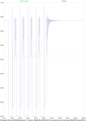
AL-0020-04E LTSpice: The smallest ripple occurs with C1 = 0pF. A placeholder part should be fitted on the PCB in case a capacitor is required.
I have only tested the circuit at +-250mV square wave input.
------------------------------------------------------------------------------------------
SiMetrix - Free limited capacity version.
AL-0017-01F The circuit is a more conventional peak detector, with C2 removed. The circuit does not work well down to 10 mV peak to peak, though it is faster than the circuit further above.
Substituting the diodes for Schottky diodes will allow this low-voltage circuit to work with bigger signals, but the discharge resistor can not be so high. This particular circuit is more suitable, consequently.

AL-0017-01F 1V peak-detector 100Hz. ~4 mV ripple and no apparent overshoot.


AL-0017-01F 10mV peak-detector 100Hz. The first cycle has an overshoot of ~1 mV, so capacitors around the op-amp need to be added or changed.

The circuit appears to be consistent to <1mV with an offset within the tolerance of the operational amplifier in this case, 8mV. This is a model, and C1 may be too small when real circuit board parasitic capacitances are included. This circuit is improved further for small signals if R1 is reduced to 470K.
An output buffer is not shown fitting, because that would make the circuit too big for this free version of the modelling tool to simulate. In any case, circuits should be kept small so that modelling is completed in good time.
The circuit is now quite good for this type of circuit. The circuit is probably good enough if the input slew rate, bandwidth is limited. But increasing the rise and fall time from 50u/s to 500u/s has only a small benefit.
 AL-0017-05B This could be better or worse because the gain is not 1+feedback as in the previous circuit, but -feedback factor solely. That is the rise time is limited by R1, R2 and C1 a little more.
 The limitations of this free version of SiMetrix, which is very good for modelling power transistors, are limiting in this case if an output buffer is required, the circuit becomes too big. On the other hand, SiMetrix is a very intuitive, easy-to-use tool.
 |
AL-0017-05B 2V peak to detector - has 4 mV ripple. The circuit is now faster because there is no gain in the circuit, and because of some changes. It is best to not combine the peak detector stage with amplification. That has always been good advice, but the old advice to avoid letting the op-amps' output saturate at either supply is now not important, modern op-amps are different to much older op-amps, which recovered from over drive slowly. |
 |
| AL-0017-05B 10 mV peak to detector - has 250 uV ripple. |
There is always value in having a theory, but a theory will be difficult to write or say until it answers enough questions and the engineer's mind is clearer about what is happening. But it is necessary to use your feeling for a design and to find a way to express what you have found in imprecise words like, reckon and as-if. Do say and ask someone, I do understand, but please help me express it in a better way.


AL-0017-09A - 2V peak to detector - has 5 mV ripple, no overshoot.
---------------------------------------
Tina TI - Putting two peak detectors together to record the greater of the positive and negative peak detectors.
See separate page, Pos Neg Peak detector circuits and models

AL-0018-02L small tidy up, so R3 removed R5 does the job. The combined two peak detectors interact unfortunately. +-25mV 100Hz square wave, gain ~31.
 |
| AL-0018-05A, but the output series resistor R5 is 220R instead of 10R (AL-0018-02L). |
The peak detector is now not so bad, and is slower and slightly overdamped. That is the overshoot that came about when the two peak detectors were combined was mitigated somewhat by R5 (was R3 and R5) being increased in value from 10R to 220R. There is little difference between this graph and AL-0018-06A, which I have not included. The two peak detectors interact, and this is not a good circuit and somewhat unexpected.

Many variations have been tested, and versions including the more complicated feedback variant AL-0018-06C, is posted left. It is based on circuits further above, but has overshoot just the same, of 60mV~, but undershoots if R5 is increased to 220R.
There is an unresolved fault in this model when the input is increased from 20 mV to 25 mV, which causes the output voltage to increase greatly. Looking at earlier graphs at 25 mV input, but with different R5, the circuit did work, so it may be that this op-amp does not work well when overdriven.

The combined output is different to a peak to peak detector shown right, which requires a greater supply voltage. This circuit function is different, but in addition, there is no path for interaction between the two peak detectors.
AL-0017-08B peak-peak detector. This circuit is too big to model on this free simulator, SiMetrix. The outputs would be summed using an instrumentation amplifier, which need not be included in this model. Instrumentation Amplifiers generally need a greater supply voltage, which is explained well in a graph in their data sheet.
AL-0017-08B peak-peak detector. This circuit is too big to model on this free simulator, SiMetrix. The outputs would be summed using an instrumentation amplifier, which need not be included in this model. Instrumentation Amplifiers generally need a greater supply voltage, which is explained well in a graph in their data sheet.
The next step
Might be to use an active rectifier follower with a single peak detector. This would be a safe rather than a novel solution. It is also likely that the error observed is not an interaction between the two peak detectors but due to an initial offset caused by including the very high impedance vibration sensor's series resistance in the circuit.
-----------------------------------------------------
Rectified approximately mean rectifier or averaged peak-peak detector
Required to process a capacitive moisture sensor. The circuit's function changes depending on the amplitude of the signal; in addition, it is faster and has no overshoot issue because there are no active components (op-amps) in the circuit.
 | |||||||
Traditional precision rectifier A smoothing capacitor should be fitted across R5 Below, R1 C4 represent a humidity sensor. HIH6030-021-001 <£10, SPI or I2C output. 246-5637 RS stock number < £2.50 capacitive element. 1V peak sine wave, 1 KHz, impedance 6M to 2K for 20 to 95% humidity at 25'C. HS1101LF TE, <£8.50, 10V peak sine wave, 0.31pf/1%RH (31pF). 180pF at 55%RH. 10KHz (5KHz - 300KHz) |


AL-0057-03A Two voltage-doubling rectifiers, one cancelling out the temperature coefficient of the other. The two outputs are combined (Vout+) - (Vout-) to cancel some of the ripple voltage. The curves are approximately 0%, 50% and 100% humidity.
- Create the .include with the model file path. The '.' makes it a spice directive rather than a text comment.
- Select a part from the library and ALT-right-click. Not right click, which lets you change the part to another in the built-in library, but so you can use a standard symbol with a new part.
- Change; prefix to 'X', and change the value to the exact model name, such as '1PS66SB82'. That name is in the file, which is a text file that may have many part definitions.
- Finally, check that the symbol pin out is correct or try again, but use an automatically generated symbol; they are usually correct.
The Schottky diodes operate with a lower forward voltage drop but offer no advantage because their temperature coefficients are the same, about -2mV/'C as silicon signal diodes. But they need to be operated at a higher current to minimise the effect of their high reverse leakage current of 3uA at 85 °C in this example. Therefore, conventional silicone signal diodes would be a better choice, which have much smaller leakage current of the order of 500pA at 85 °C.
Operating the diodes at lower current, though, reduces the forward voltage drop, but I used the calculator link below, but I got the wrong answers.
 |
| £20, 1970s Mulimeter's lowest ranges are 250mV DC, 1.5V AC at 50K ohms/V DC and 10K ohms/V AC. You can see that the red AC Voltage scale is only slightly non-linear compared to the black DC ranges. The movement is therefore <20uA, I think it is about 15uA and <<250mV? The multimeter's movement is protected by two silicon diodes connected in anti-parallel, but the AC voltage measurement uses the lower voltage drop germanium diodes. The answer is probably that the multimeter's accuracy is not so good. |

AL-0058-01A Fully wave mean detector. The signal amplitude is about a quarter of the first circuit, so the gain of the amplifier is higher. An instrumentation amplifier such as AD8293G80 would do a better job.
Many spice models from different manufacturers work in many simulation tools, including LTSpice.
----------------------------------------------------
What can be concluded?
Almost certainly, different combinations of things shown could improve these circuits further. But there is some point where refinement is enough, and the designer must stop and move on to the next problem. That is still going a little further [tinker a bit] than necessary to be sure of what you have done, then stop and move on to the next thing to do.
The TED talk linked below is interesting. The speaker discusses how it is necessary to be open to trying many things (procrastinate, he says) to be a successful original thinker. I think the speaker is coming at Temperament (that I discuss on my website), but in another way.
The TED talk linked below is interesting. The speaker discusses how it is necessary to be open to trying many things (procrastinate, he says) to be a successful original thinker. I think the speaker is coming at Temperament (that I discuss on my website), but in another way.
No comments:
Post a Comment