Sunday 1 July 2018

Electronics - High frequency metal vapour arc lamp power supply

Changed; 16-04-2024, 15-04-2024

A reliable high-frequency ballast for a metal vapour arc lamp was made long ago.  It works similarly to a conventional 50Hz mains power source and choke but works at a high-frequency regulated AC current source instead.  It uses variable frequency to tune the L.C resonant circuit to create the high voltage necessary to strike the arc lamp.  This power supply is rated at 1A for a Spectral Lamp made by Osram. 

Images in Blogger are limited resolution.  Click or right-click to view the image with a good definition. 

Summary
I have given myself a design objective to improve the power supply efficiently and to update the parts used.  The Arc-lamp power supply design involves a lot of iterations of various models.  The requirement is unusual in that starting up voltage and power circulating in the power supply and the lamp is very high for a few seconds, then drops and runs at 150mA until the voltage falls further and the current rises to 1A until it fully warms up after several minutes.  After starting and warming up the unit needs to run efficiently at 10-60W depending on the spectral lamp type chosen. 


In this case, it was useful to get a functioning though inefficient, robust design to work to prove the design idea and the understanding of the lamp.  There were many design iterations that I have not included.  By using a newer MOSFET transistor type and the switch mode power supply type to a resonant mode the transistor losses should improve.  The power supply shuts down and restart if the lamp fails or is not fitted.

Conventional mains frequency ballast;
The metal vapour arc lamp arc is struck with a high voltage of 900V peak (GE fluorescent tube starter data sheet) and in the high-frequency lamp, a limit was set at 1.5KV peak which works reliably.  The noble gases ionize and begin conducting current.  In the case of Sodium (Na), lamp voltage quickly drops to 500V and then operates at 100V for a short time, heating up the metal until it becomes a vapour within the lamp.  During this short period, it is likely that the lamp unit will behave like a spark-gap transmitter.  The lamp voltage then falls to about 15V at 1A as the metal vapour conducts current and the lamp appears to have a resistive characteristic.

The mains lamp unit appears to re-strike each mains cycle 2x 50Hz so could cause emissions all the running time that can be observed with an oscilloscope or a spectrum analyser.  You can also observe some blue and flickering light the re-striking causes in a low-frequency ballast system.

I found this video on YouTube of a sodium vapour arc lamp starting.  You will see 
some blue and other colours around the electrodes plus flicker and fluctuation in this 
conventional mains power ballast when it is fully warmed up and running normally. 

When warmed up and running normally blue and other colours plus flicker and fluctuation are much less evident in the fully warmed up high-frequency metal vapour-arc-lamp power supply.  The circuit below is different from modern electronic ballast lighting in that the lamp's light is constant and regulated, that is, the current waveform is not modulated by rectified AC mains voltage but by 2x 50 KHz or whatever the running frequency which makes this sodium arc lamp in the video behave as a resistive load.  So it will display no doubt flicker still but with fewer other colours because other noble gases used to start the lamp are evidently not activated.

Starting with guesswork then developing a sound theory leads to a robust solution;
The starting and running characteristics were all discovered by observation and experimentation, as described above, but with a range of different metal arc lamps.  The data sheet on the lamps has little information.  Because the lamp voltages range from 10 to 60V the current range is at least +-12% with other tolerances = 100% * 50V/240V + other tolerances.  I set the starting current low but high enough to cause the lamp to warm up. 

The concluded design is a simpler solution.  This is often the way the thing turns out that the final simplicity conceals the effort necessary to achieve it.

Heath Robinson - drew cartoons of elaborate machines but engineers should make machines 
to function well in an uncomplicated way from a range of imprecise materials and parts.  I 
think Heath Robinson showed in fiction a desire for complicated machines as toys. 

It is reasonable to start a project and expect it to first be overly complicated but this does not have to be so and I have constrained my designs from the start.  In due course, the design and the function should become simpler and plainer for the user to use.  I have observed designs that present too many complications that are not liked by the customers and the company eventually simplifies the design so it is more like an earlier model but the problem is for the company to recognise the problem.

It is not an uncommon problem for small companies and individuals to have difficulty in getting support from big companies on products those companies make.  Many parts made by big companies may not be available to other customers but it can be worth asking about them.  But also many very big companies are particularly supportive of small companies and individuals.  There has been a positive change since the 1990s with big companies helping small companies and individuals much more although some never stopped and have always worked that way.

Spectral-lamp
Laboratory spectral lamp unit

Half-bridge - switch mode vapour arc-lamp power supply;

Based on a successful design but with changes and using newer parts than were fitted in the actual lamp power supply in the early 1990s.  The lamp and power supply are enclosed within a metal box with metallic contact on all edges to the lid.  There is an aperture for the light to exit - this provided the lowest emissions in conducted EMC test up to 30 MHz at that time.

Since working on this project I have worked for automotive contractors one of which had a test chamber, LISN (line impedance stabilisation network) and a large field test site.  It is possible to use a LISN and analyser up to 150 MHz - although uncalibrated this will make initial testing more practical.  Using an oscilloscope is an essential first step to look at the diode overshoot which is the diode turn-on time and may cause EMI.  Measure the width of the overshoot if it is say 10 ns (half a cycle) then any related to the diode emission is likely about 50 MHz.

The most significant thing about using a LISN is that you do not just measure conducted emissions but you also get a good indication of potential radiated emissions without needing to leave your workspace and equipment. 

Some of the spectral lamps could behave as a spark gap transmitter.  This is why the output choke should be a low Q filter type but R13 also achieves a similarly low Q.
  The mains power supply AL-0026-01D (6).  The power supply has components rated for 200W 
or more briefly although the lamp power is much less when it is warmed up.  C4 was fitted across
 the source current sense resistor on the PCB but on reflection, this may be counterproductive to 
fit if it extends the switching moment pulse outside any dead-band filter included in the controller? 
  • C4 - slightly compromises the dead-band turn-on noise filter but beneficially should reduce the chance of high voltage transients in the Source pin compromising the gate driver.   In any case, the driver chosen is much more robust and can withstand 100V <300nS than the original driver IR2111 which had lower over-voltage ratings.  Even so, it was adequately robust.  
This circuit is a little different and is not finalised but the original was working well and reliably for a decade of daily use. 
  • The circuit above does not work over the full voltage range and lamp power rating.  But the regulation will cease if the mains voltage drops to 150Vac depending on the maximum power 60V Helium lamp.  But from the models below the circuit may continue to work down to 100 Vac if the power supply were to run at close to but just a little above the resonant frequency.  That is although the Q of the resonant circuit would be low it would still create a higher voltage than the incoming supply voltage.  Operating slightly above resonant frequency so that the transistors switch on at zero inductor voltage and therefore more efficiently.  That is the high currents seen in the models below do not occur.
  • The Status LEDs for starting could be supplemented with a status LED for in-regulation.  See controller diagram sheet 5 in pdf; AL-0026-06A.pdf
C16 & L2 form a tuned circuit to create the high voltage necessary to strike the vapour arc lamp's arc.  The frequency first reduces to below resonant frequency of 50 KHz to maintain about 150mA until the frequency drops to 50 KHz.  The circuit then runs at 50 KHz and the current in the lamp current increases until it is controlled at 1A by pulse width modulation.  A change that needs to be made is that the frequency needs to settle operating just above resonance similarly to the ballast controller ICs further below.

Revised for 50 KHz operation a smaller inductor L2 (100uH) has been selected.  The resonant frequency for striking the arc is now 87 KHz (C12=33nF) and L1 protects the circuit from damage when the arc is struck.  Note that although L2 is physically smaller and the originals got hot, the manufacturer's models are very accurate, although the working voltage of 2,000V may be too high for the part it should be possible to evaluate with that part then have a special choke with better interwinding insulation.  The change to this strategy would be to reduce the frequency ramping or not use the frequency ramping for starting but keep the starting circuit in place to accommodate choke inductance changed with power throughput. 
 
A fairly large difference between the starting high frequency and lower running frequency was designed in, to moderate the starting up power in the lamp which in any case was still high at roughly 75W = 150mA * 500V or 150W = 1A * 150V for a 15W rated sodium lamp.
 
The controller and half-bridge have an added high lamp voltage sense to reduce the power as the lamp voltage increases.  There is also a Zener diode added to allow 10% current when the lamp strikes and first starts to warm up.  This still might be an excessive current? See controller and half-bridge sheets; AL-0026-06A.pdf

The current mode switch mode power supply controller works well in this simple current output design providing some of the current regulation, particularly for mains 100 Hz ripple on the power supply.  There is a conventional slower outer control to set the lamp current accurately that responds as fast as is practical.  The operation is unsymmetrical the negative pulse width is shorter, higher and set by the controller, and the longer positive pulse completes the remainder of the period of oscillation.  The controller also includes over-voltage shutdown in case the lamp is an open circuit such as if it is not fitted.  The over-voltage is sampled on the positive peak and the limit is set at about 1,500V peak, the peak voltage will be a little higher than this, so the capacitors are rated at 2,000V but the inductor's voltage rating would need to be confirmed.  The lamp's light output and life appear to be very good is more uniform light noticeably at each electrode where you see fluctuation and ran reliably daily for at least a decade.

The circuit operating frequency ramps through L2 & C16's resonance which causes the high voltage necessary for the lamp to strike which is more like how a leakage transformer rather than a fluorescent tube starter operates.  Otherwise, the circuit operates in a similar way to how the conventional 50Hz choke ballast above works.  When the lamp is at full temperature C12's purpose is mostly complete although it may provide some filtering of RF emissions.  L2 provides a 1A average current source for the lamp.  Spectral Lamps require 10 to 60V at 1A RMS depending on the lamp metal.  The lamp was plugged into a ceramic B9A valve base, called PICO 9.

Using average current instead of true RMS current introduces an error.  The current waveforms are a mixture of rounded sine, triangle, sawtooth and square waves but using a multiplication factor of 1.1 would be about right and is accurate as is required.

So for an; (RMS/Average)
Sine wave; 1.11 = 0.707/0.635
Square wave; 1.0   = 1.0/1.0
Triangle or sawtooth; 1.15 = 0.577/0.5

Multiply the average value by 1.1 to approximate the RMS value required.


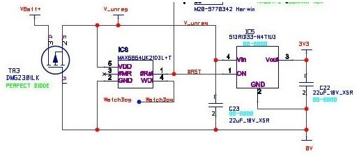
Low Voltage Power Supply

AL-0026-01D (4) low voltage power supply.  Just enough power will be supplied from the current sensing when the lamp is drawing the rated 1A to run the low-voltage circuit. 

A mains voltage 2-3mA PTC could not be found now so a higher power rating transistor has been selected instead.  
  • Raising the value of R23 to 47K so that if the lamp does not start the power supply shuts down may be practical but the value will need to be experimented to be found? The gate driver's shutdown pin is wired in but even so, the operation needs to be checked?
  • R23, 22K should provide 2mA at 100V, enough to start for 50 seconds but not run.
This part of the design is not fully optimised.  N2 is the neutral half-wave filtered mains voltage input therefore the power wasted is better than halved at <1.4W in the start-up condition. 


Assessment of the original arc-lamp power supply;
The power consumption of the whole power supply was fairly high but what mattered was that the lamp was an excellent source of flicker-free and low-ripple light.  The main inductor which is about 40 x 40 x 40mm depending on which was used ran hot or very hot depending on which one was used.  The transistors were each mounted to PCB mounting heat sinks rated at about 15'C/W each and they ran cool.
  • Increase the size of the inductor or increase the frequency of operation to reduce power loss or at least to reduce the inductor's temperature rise.
  • But regulations were coming in that required electrical equipment to have power factor correction if the power was greater than 75W.  In addition, sodium street lamps if only sodium light was required are better priced and lamp life with this option is longer but street lamps use more power and produce more light than a sodium Na Spectral lamp. {STM data sheet says this amounts to 25W maximum lamp - which varies with other advice}.
  • Consequently, if the full range of Spectral Lamps are supported then provided the power supply's efficiency is improved then no power factor correction circuit needs to be added.  That is because the highest power-rated spectral lamp is Helium (HE) which is rated at 60W.
  • The operating frequency has been increased to 50KHz and the starting frequency resonance of 70KHz to start at up to 100KHz. 

Earlier designs often destroyed transistors at start-up;
When the arc was struck the output transistors were often destroyed.  My design assumption was that this would not happen because there would be enough stray inductance for the C16 discharge current to be limited the current adequately was wrong.  Secondly, the circuit for the arc-lamp current path was far from the power transistors and I could not see a path on the PCB that was nearby either to explain this.  Although the current sense transformer did carry the high discharge current nothing was damaged in that circuit's path.  L1 was added although in that location about 4u7H or 220mR wire wound resistor adequately resolved the issue -  for such a small impedance to be significant then evidently the current pulse was very high and fast.

Op-amp unstable;
The dual op-amp in the controller section could be unstable due to the electromagnetic emissions from the power inductor.  A workaround is to add a 100uF or more likely lower capacitance to the output - so that it is overcompensating.  The data sheet recommends loading the output with a pull-up resistor to draw more current.  A capacitor is shown on the circuit diagram.

Another option is to also place the Op-amp some distance from the power parts and under the PCB.  Hopefully, the screening will be adequate so that the amplifier does not need to be placed on the bottom layer of the PCB?  The design has been changed to an SMT design which may also allow us to separate the input inductive filter from the output choke by distance plus better screening using 0V and power planes 5V1+, or Vc+.
 
Op-amps and other circuits within switch mode power supply controllers intentionally have greater charge storage at the pins I read recently. 

Power Input filter;
The input filter circuit with the safe X and Y class capacitors has changed a little since about 1985 other than to become required standard practice to fit rather than being optional.  Some of the parts shown will also need to be reviewed.
Input filtering AL-0026-01D (3) - there is only a single point connection 0V to Earth connection although bonding at 
many points would be better - this cannot be done for safety reasons one single point RF  connection is achieved by 
commonly available safety-approved type Y-class capacitor.  In any case, the star point strategy works fine with care.

The input filter circuit is compromised for safety in that there is a single bond 0V to Earth via the Y-class capacitor.  I have considered a more efficient design that includes an output transformer but I have not pursued that further.  With that design one of the lamp supply voltage connections is connected to Earth for potentially lower Electromagnetic emissions (EMI).

The Earth and Neutral connections have two resistors in a series to discharge C3, the discharge would be safe but is likely to cause complaint.   The addition of these resistors does compromise safety and the particular types chosen should be checked for their suitability.   Without those resistors, the discharge energy is safely within the standards and those resistors could be omitted. 

AL-0026-01D (5) control circuit.  This circuit is wrong or has incorrect component values. 
The Red LED flashes during starting and is stead on when warming up and also running.
  • The left circuit creates the slow voltage ramps that modulate the Switch mode power supply oscillator frequency.  When the lamp is struck and 150mA of lamp current is reached then the ramp stops and the frequency drops until the lowest frequency about 50KHz is reached and then the current rises to 1A and the pulse width modulator starts to control the current.  When the lamp current has risen to 1A there is enough current from the current transformer to run the low-voltage circuit so the wastage from the mains ceases. 
  • The right-hand circuit is the switch mode power supply circuit.  The IC chosen is a low-power version of a 1980s Unitrode Current mode controller that was stable in this application even without a small element of Voltage mode control added. 

ALTERNATIVELY;  (simplification)

  • Select components that will resonate at about the operating frequency.  The supply voltage can be set high enough that the Q can be low and the LC mis-tuned but still attain 1,500V to strike the arc.  
    • If the chokes value reduces by, say, 20% then the frequency could be set 10% higher in future the variable frequency starting circuit might be removed?
  • Modelled below with L2 = 100uH then C12 = 100nF for 50KHz.  This circuit can run with 100Vdc supply even though the lamp voltage is 120V - 150V pk-pk.
  • This alternative could be tried by changing C12 and removing D12.  This will likely work even with a lower voltage supply but in any case, PFC that will boost the supply voltage is required.
A different controller with many more functions integrated could be used such as; TEA19161T/2,  TEA2016AAT these use a half-bridge driving into a transformer with leakage inductance so a PFC section may not be required. 
  • Burst mode would need to be deactivated.  I have not investigated if these ICs will work, they work in voltage mode but they are efficient.
AL-0026-06A.pdf does not yet incorporate all the changes but does show a different method of current reduction when the lamp is starting.  Another change might be to start the lamp at slightly lower frequency than the running frequency.  A better strategy would be to use a fluorescent tube/arc lamp high frequency ballast controller.
AL-0026-01D (2) Block diagram. 

It is most likely that the running power consumption will be up to 65W but if it turns out to be 70W such as with a He. lamp then a PFC will need to be added in case 75W were exceeded.  Most lamps though are lower powered and the whole unit's power should be below 20W with many lamps such as Sodium Na.   It depends on how much better efficiency newer chokes turn out to be compared to what was available or could be wound in the 1990s?  Some of the chokes modelled further down in this blog are much better.

Notes Mods and ToDos AL-0026-01D.  PDF of all pages of the circuit design.
 
------------------------------------------------------------------------- 
  
Developing and refining this 1990's design

The circuit is very similar to the working original circuit.  There are several incorrect parts such as connectors put down and develop the ideas without being distracted by detail.  Polypropylene and Polycarbonate power capacitors will need to be changed to Greener RoHS-compliant types.
  • There was an earlier stage that amounted to play that was very important.
  • A step-up high leakage, high frequency transformer did not work well I struggled with the design which a Mullard field applications engineer suggested and supported me with. 
  • An earlier working design included a full-bridge 24V DC, which worked well. 
  • A mains voltage full bridge also worked well but was unnecessarily complicated.  I did a lot of work with this design.

  Revision;
 
Output transistors - first look;
The original circuit used IRF841 transistors plus PCB-mounted heat sinks each for the half-bridge output.  Although the newer transistors below also include an avalanche diode and the diode has a reasonable switching time the switching losses could be a significant factor.  That original circuit had a transistor current limit of 4A.
  • A rough estimate for the candidate's new transistor power can be done using Ron.
  • If the transistors are soldered to PCB with no additional heat-sinking then the package dissipation is 62'C/W.  That figure depends a lot on the mounting orientation of the PCB.
The top transistor's Drain is soldered to an area of copper for additional heat sinking.  I have included a lot of decoupling to minimise EMI radiated by this pad which is connected to the positive supply.  As discussed below a PTC thermistor to sense over temperature and shut down the controller could be placed in this area.

The bottom transistor's Drain is soldered to an area of copper for additional heat sinking.  However, the copper area will cause EMI to radiate and it will be necessary to experiment with snubbing and switching time to minimise EMI adequately.  The bottom transistor conducts high and shorter current pulses (although the maximum current is not as high as might seem at first).

https://electronics.stackexchange.com/questions/26783/how-do-i-determine-the-area-of-copper-needed-on-a-pcb-to-provide-adequate-heatsi?utm_medium=organic&utm_source=google_rich_qa&utm_campaign=google_rich_qa 

This example with 50mm x 50mm on one side of the board but with a smaller transistor would improve the thermal cost-efficiency to better than 35 'C/W.

----- Return to the transistor power selection later -----

Simulation to show basic circuit operation;
Simulation adds a step but gives me more insight into the operation of the circuit before proceeding to have a PCB made.  This model will confirm or remind me of assumptions and calculations made previously. 
AL-0028-07B, SiMetrix 9.1 simulations of the output choke/filter and the lamp represented by the 
bridge rectifier and resistor in this case and a voltage clamp in other cases.  Top right is the current
transformer monitors average current as an approximation to RMS current. 
  • The current transformer is; 1:150, therefore R2 = 150R gives a 1V per amp average but the waveform is not square, triangular, sawtooth or other but complex and I have not been able to estimate the RMS current using the power measurement probe in SiMetrix.  However, I am hoping to find a value that is near enough using the average value scaled.  The mains frequency choke ballast would have no regulator but for a 110VAC and 230VAC switch, so the higher power lamps probably should be running at a lower current.
AL-0028-07B lamp; 15V 1A into 1 ohm.
    • The Voltage offset is due to the duty cycle 96% was adjusted until the power looked about right at 15W.
Waveforms are ripply because the circuit includes capacitors with significant reactance. 

Purple - Filter voltage.  The coupling capacitor's voltage is 200V and a 500V part may be substituted.
I-sens = current transformer rectified voltage (across 150R), 0.8V.
Brown - I-Probe Drive Transistors, +1A to -2.5A
Blue - Lamp Voltage, ~11V.
Red - Rectified Average lamp voltage (12V).
Green - Power in load resistor R1, difficult to determine ~15W? 
---------------------------------------------------------

AL-0028-08B is a similar circuit as -07? but the lamp voltage is; 
60V and R1 = 60R, the highest power lamp.

Purple - Filter Voltage.
I-sens = current transformer rectified voltage across 150R, 1V/Amp average.
Brown/Green Probe 1 Mauve = Transistors Current, +2.5A -4.5A.
 Green - Lamp Voltage, 60V?
Green - Power in output load R1.  Looks very high >100W but that looks wrong.
Red = Rectified smoothed Lamp-V R1, 60 ohms, 60V. 
      • The duty cycle is 87% 
  • Simulation of an arc lamp warming up assuming the lamp is behaving resistively.
-----------------------------------------------------------------------------

AL-0028-09B 60V 1A from 110VDC minimum V+, duty cycle 50%.  Same circuit as version -07?
With a 220uF reservoir capacitor, 90Vac, 60 Hz minimum is required.

Purple - Filter Voltage.
I-sens = current transformer rectified voltage. 0.9V
Probe 1 Brown = Transistors Current, +2A -2A. 
 Green - Lamp Voltage.
Green - Power in load R1,  >60W?
Red = Rectified smoothed Lamp-V,  60 ohms.
  • The power supply is running flat out therefore there is no regulation.  So anticipate double mains frequency fluctuation in the light output.  So double mains frequency fluctuation in the light output is to be anticipated. 
    • This issue can be resolved by adding a Power Factor Controller (PFC) or a voltage doubler rectifier switch.
A resistor may need to be added across L2 to stop it from ringing, the part should not be fitted unless it is found necessary.  C1 when reduced caused the peak current to increase from 4-5A to 7-8A, that is its reactance is significant and C1 was increased from 220nF to 470nF. 
  • AL-0028-07A Graph  Old version C1=220nF, 15V 1A, 400Vdc - peak current is okay.
  • AL-0028-08A Graph  Old version C1=220nF, 60V 1A, 400Vdc - high peak current.
  • AL-0028-09A Graph  Old version C1=220nF, 60V 1A, 100Vdc - peak current is okay.
  • Status LEDs have been added to this revised power supply particularly relevant is the controller page See pdf; AL -0026-06A
Q of L2 an RF filter choke should be quite low.  In any case, a soft magnetic should be chosen which has a low Q because when the lamp starts and is warming up the lamp is likely to behave like a spark-gap transmitter.  But when it is warmed up it should behave resistively and tests tend to confirm this.
  • Using average current rather than the RMS current worked well and is about right for an approximate triangle wave.


If the higher-power lamps operate as an arc when fully warmed up;

If the higher voltage lamps operate as an arc rather than a conducting metal as the Sodium lamp does, which is most likely,  then the circuit will work regulated at low voltage, with high circulating current but without PFC.


L1=100uH, C1=470nF, 60V 1A;
  • And for a 15V lamp at 400Vdc +1A to -2.5A (AL-0028-07B above)

Consider adding Power Factor correction to improve regulation and efficiency over the working voltage;

AL-0053-01A High-Frequency Arc Lamp power supply with PFC
Power Factor correction function added. 

This PFC would always provide a higher DC voltage than the rectified mains peak-to-peak voltage whereas the configuration below can provide more than or less than the peak-to-peak mains input voltage.  The voltage out could be variable based on the measured lamp voltage plus the reservoir capacitor minimum voltage but always less than 450Vdc. 
AL-0053-01A (3) Power Factor Correction buck-boost (Full Bridge).  Arbitrary value components are shown.
Provides a high enough voltage to power a lamp without excessive voltage that would be inefficient.  About 30Vdc to 150Vdc + Reservoir capacitor ripple amplitude.  The drawback is that I have not found a suitable controller and using logic to switch modes between buck and boost would put a little glitch in the current drawn.  The glitch could possibly be minimised by using a current mode controller.

The risk is that current mode controllers often have a dead period to prevent current glitches from upsetting the control.

A current mode PFC may satisfactorily transition between buck and boost more smoothly; L4984D, L6562A, TEA19162.

Buck-boost PFC control strategy draft;
If the input voltage is greater than the output voltage then the PFC works in buck mode. Otherwise the PFC works in boost mode.

  • Buck mode - the top transistor is switched by the controller.  The bottom transistor is switched off.
  • Boost mode - the bottom transistor is switched by the controller.  Ideally, the top transistor should be switched on but it will need to be switched off and then on at the beginning of the PWM on cycle to recharge the gate driver boost power supply.


The lamp power supply - considering the modelling further above;
  • Consider removing the power from the current transformer and using power from PFC for low-voltage sections. 
  • Changed output L, C & C to 470uH, 100nF + 6n8F.  As, AL-0028-07A,  AL-0028-08A, AL-0028-09A.
  • Reduce the size of the reservoir capacitor to; 50uF.  Remove the choke that is between the rectifier and the half-bridge output. 
  • This change reduces the peak current in the transistors and improves the light output regulation. 
  • The poor regulation warning circuit and RED LED is not required.  There is always adequate power for the regulation to be good, when everything is in order, with the PFC option included. 

AL-0028-10A 60V 1A from >=400VDC PFC,  duty cycle 72%.  Same basic circuit as -07? 
The inductor is larger and more expensive but should result in less power loss. 470uH, 100nF & 6n8F.  Starting Resonance 87KHz.

Purple - Filter Voltage.
I-sens = current transformer rectified voltage. 1V
Probe 1 Brown = Transistors Current, +2A -2.5A. 
Green - Lamp Voltage. 
Green - Power in load R1,  >60W?
Red = Rectified smoothed Lamp-V,  60 ohms.


Modelling a switch-mode power supply without using simulation tools is also relevant;
An inverter needs to be placed between the output and the gate driver because the controlled current is sensed in the bottom transistor.  There is an inverted output controller UC3847 that was used before but it consumes more power at up to 21mA.   

Consequently using an estimation of minimum on-time based on square law to consider increasing the operating frequency is a useful modelling exercise.  The next output transition (minimum PWM on time) is determined by the time between the current flowing into the substrate diode in that transistor (current flowing out of the inductor but not conducted by the MOSFET) must be at least tRR (~200nS).

Conclusions for the simulation of general operation above;

Lowering the Q of L2 by adding R3 to reduce ringing when the lamp is behaving as an arc should reduce RF emissions.

It is unlikely that this extra design step would be assisted in the design process application notes generally do a good job of explaining standard topologies.  But modelling the power in the transistors is likely to be beneficial - I had been advised that would be the case!

      Simulation for power supply running at near L.C resonance;

      The simulation below now considers the switching power but does not include changes with temperature increase.  It will, therefore, underestimate power consumption because Ron increases with temperature rise so, therefore, the power dissipated increases with temperature. 
       
      This simulation does not take account of the change in resonant frequency due to inductor L1's inductance reduction with power throughput.  The operating frequency probably needs to be increased by 10% if the inductor value drops by 20%.
       
      AL-0054-09A - Lower Ron transistors and a higher current gate 
      driver are used.  400Vdc minimum from a PFC boost section.

      LTspice's available parts were used mainly because making them is fiddly hence I've used the library 20:1 current transformer.  This is a new more comprehensive simulation using LTspice 24.x - replacing the old SiMetrix model does not run now.  The power MOSFETs were created using the LTspice nmos part and changing the model to the manufacturer's model. 

      LTspice alternate solver was used and the simulation was 800uS to 1mS for measurements, with the maximum time step 2-5ns.  Ton is adjusted until Vav = ~0.9V

      Gate resistors increased to 100R, diode gate clamp was added this value is almost certainly too high for efficient operation.  A snubber is required even so the peak currents and power losses without one are okay.

      The .meas directive should give 100% accurate results I am told.  But have not found how to use .meas but I do not need to use it.  I have made more mistakes, resulting in wrong results, as a consequence of reading LTspice instructions.  They are clear but often short of the required detail.
       
      The new snubber values 220pF and 22R have not been modelled below but there would be a small increase in the peak currents in some cases.

      AL-0054-05B 400Vdc, L1 = 100uH, C3 = 33nF, C2 =470nF, 60V Zener load

      Power measurements; 

      Isense 20R = 80mW,  Vav = 935mV,  Pulse width; 1.55us in 20us. 

      Gate driver; U1 = 22mW,  Top Transistor; M1 = 628mW,  Bottom Transistor; M2 = 2.6W. 

      Currents; IL1 = 4.6A to 2.1A,  MOSFET currents are 12.2A to 12.9A 

      AL-0054-06B 15 Ohm resistor load.  400Vdc,  L1 = 100uH, C3 = 33nF, C2 =470nF.

      Power measurements; 

      Isense 20R = 46.9mW, Vav = 882mV.  Pulse width; 1.0us in 20us. Lamp 15W

      Power; gate driver; U1 =  21mW,  Top Transistor; M1 = 59mW,  Bottom Transistor; M2 = 301mW. 

       Currents; IL1 = 2.9A to 1.16A,  MOSFET currents are;  +-2.9A

      AL-0054-07B  150Vdc. L1 = 100uH, C3 = 33nF, C2 =470nF, 60V Zenner load

      Power measurements; 

      Isense 20R = 69mW and 59mWrms, Vav = 886mV.  Pulse width; 3.75us in 20us.

      Power; gate driver; U1 =  21mW,  Top Transistor; M1 = 1.0W,  Bottom Transistor; M2 = 421W. 

      Currents; IL1 = 3.3A to 2.0A,  MOSFET currents are 11A and -12A. 

      AL-0054-08B Into 60V zener diode load, 220uH + 470nF + 15nF, 400Vdc.

      Power measurements; 

      Isense 20R = 71mW, Vav = 923mV.  Pulse width; 2.5us in 20us.

      Power; gate driver; U1 =  21mW,  Top Transistor; M1 = 134mW,  Bottom Transistor; M2 = 400mW. 

      Currents; IL1 = 1.1A to 3.2A,  MOSFET currents +-3.1A. 

      Maximum power (50% duty model below);

      • With 47uH at 100V and 60R does not achieve the required power predictably and actually. but with 100uH and 60V Zener diode load does achieve the power.  It may be possible to run this power level without a boost PFC.
      • With 470uH at 400V and 60R does achieve the required power and the inductor could be reduced to 330uH to ensure there is adequate power.

      AL-0054-09A Into 60W resistive load, 470uH + 470nF + 6.8nF, 400Vdc.

      Power measurements;  

      Isense 20R = 56mW, Vav = 942mV.  Pulse width; 2.5us in 20us. 

      Power; gate driver; U1 =  21mW,  Top Transistor; M1 = 160mW,  Bottom Transistor; M2 = 228mW.  

      Currents; IL1 = 1.6A to 2.0A,  MOSFET currents -2.0A. 

      The required Vav = 900mV is achieved with a pulse width on time of; 7us.

      Conclusion power measurement and transistor efficiency;

      LTspice at least gives a power estimate but it looks like it is wrong because the average value Vav varies with the power in R4.  The PWM was set by measuring the Vav repeatedly until I get about 900mV.

      On the other hand, SiMetrix models AL-0026-04b and -05b do not work since SiMetrix has been updated since I made those models.  In any case, those models did not show the mean of the squares or products. 

      I have not taken the precautions mentioned in Infineon; DT-97 3 art "Managing Transients in Control IC Driven Power Stages", Method B. In any case, the original circuit was fine and the newer drivers are more robust.

      By using a lower Ron MOSFET the half-bridge becomes more efficient, confirming previous measurements and estimates.

      Because LTspice is not limited I used the gate driver model rather than a simplified model using current and voltage sources.
      • The model for the metal vapour arc lamp is changed to simply a resistor or two Zener diodes in series back to back. 
      • The objective is for the RMS current in the lamp to be 1A (+-13% I guess) which occurs when 50mW is dissipated in the sense resistor.
      • From above the average current value is a rounded mixture of sine, triangle, sawtooth and square waves and using a multiplication factor of 1.1 would be about as accurate as is required. Unfortunately, modelling does not confirm this and there is a big discrepancy in measuring the power in the sense resistor and using the Vav to set the lamp Irms.
            The lower Ron IPD60R280P7 MOSFET gives better efficiency.  But the higher current driver 2ED2184 improvement was marginal.  Both have been incorporated into the circuits above.  IPD50R280P7 would introduce greater switching losses but should be an acceptable alternative.

            Adding Schottky diodes to the gate drive did not reduce the exceptionally high gate pulses in some cases, but with the increase in Rgate to 100R the peak current was reduced to an acceptable level.  A snubber is still required though. 

            -----------------------------------------------------------------
            Evaluation of reducing the start-up frequency ramping frequency so that the ramp is enough to  bring about resonance over the range of inductor change with power through put.

            Although 150mA lamp current during starting was found adequate the method of current limiting is changed to sensing the higher lamp voltage and reducing the current proportionally but not down to zero.  This is similar to how a traditional ballast works and will surely result in shorter lamp life similar to what is quoted for the lamps.  See alternative circuit AL-0026-06A, ramp frequency for starting is still interoperated but it needs to be changed.

            I have run such a circuit from a 48V power supply and it started a sodium spectral lamp and ran fine but that was at 20KHz with a starting frequency of 50 or 70KHz?  That was using a full bridge stepper motor BIFET driver IC.  In other words, this circuit should work. 

             The circuit below is the same as above but for component values which are for operating at about resonant frequency.
             
            AL-0054-04F The operating frequency is the same as the tuned frequency of L1, C3, 
            (100uH, and 100nF, 50KHz). 

            LTspice alternate engine was used and the simulation results were taken between; 800uS to 1mS.  And the maximum time step is set to 2ns to 4ns.

            AL-0054-01E 100Vdc, L1 = 100uH, C3 = 100nF, C2 =470nF, 60V resistor load
            Power Measurements; Note no change from Zener load to a resistor was applied.

            Isense 20R = 59mW, Vav = 979mV.  Pulse width; 6.0us in 20us.

            Power; gate driver; U1 = 21mW,  Top Transistor; M1 = 754mW, Bottom Transistor; M2 = 972mW.

            Currents; IL1 = 3.2A to 4.2A,  MOSFET currents 4.2A and 4.9A

            AL-0054-02E  Into 15W resistive load. 100uH 100nF, 100Vdc.
            Power Measurements;

            Isense 20R = 58mW, Vav = 966mV.  Pulse width; 5.6u in 20uS. Lamp 19W

            Power; gate driver; U1 = 24mW,  Top Transistor; M1 = 200mW, Bottom Transistor; M2 = 414mW.

            Currents; IL1 = 2.8A to 1.9A,  MOSFET currents; 2.7A and 2.7A. 

              AL-0054-03F  Into 60W resistive load. 100uH 100nF, 100Vdc. 

            Power Measurements;

            Isense 20R = 100mW, Vav = 1.0V.  Pulse width; 4.5u in 20uS.

            Power; gate driver; U1 = 21mW,  Top Transistor; M1 = 631mW, Bottom Transistor; M2 = 1.6W

             Currents; IL1 = 3.2A to 5.5A,  MOSFET currents are -5.3A -5.5A. 

            AL-0054-04F  Into 60W Zener clamp load. 100Vdc {L.C = 100uH 100nF}
            Power Measurements;

            Isense 20R = 80mW, Vav = 941mV.  Pulse width; 6u in 20uS.

            Power; gate driver; U1 = 21mW,  Top Transistor; M1 = 612mW, Bottom Transistor; M2 = 1.1W

            Currents; IL1 = 4.3A and 3.2A,  MOSFET currents -4.8A and -4.2A. 

            Conclusion for operating at about  LC resonate frequency;

            As before, LTspice at least gives power estimates that look wrong.  The power in R4 and the average voltage vary widely, they should agree well when the arithmetic is done. 
            • The objective is for the RMS current in the lamp to be 1A (at least +-13%) which occurs when 50mW is dissipated in the sense resistor. 
            • The high circulating current could be reduced therefore efficiency improved by fitting a snubber.  The snubber should in any case be fitted.  The gate resistor 100R is almost certainly too high although it works well.
            • The efficiency could be improved by using a buck-boost PFC controller.   Although some of the chokes modelled below look much better than the working earlier power supply.  That is a good efficiency that should be expected. 
            • The current mode controller will not work with this tuned mode power supply because the current flow is not increasing during the whole of the top transistor on time at full power output. {Bottom transistor in the circuits at the top of this blog}.
            • The circuit efficiency could almost certainly be improved by using one of the zero voltage or zero current variable frequency controllers.  But I do not know if such a controller would work with a wide input voltage or if it generates the resonant frequency high voltage for starting?  That is though these controllers are usually called resonant mode controllers.

            LTspice 24 is the Analog Devices version that supersedes XVII, the last Linear Technology version
            • Where there is a part for example nmos use that part rather than the auto-generated part.
              • Change the prefix to X (for the external part) rather than NM.
              • Change the value to the exact name in the model library.
              • Remove the path and ensure the library is placed in the working directory.
              • add a .inc with the added model file name to the diagram.
            • Avoid using more than one net name for a net eg placing 0V on the reference ground plane (has a down-pointing triangle symbol). 
            • In this case, it was necessary to set the maximum time step as low as possible.
              • It is also recommended to turn the compression off.
              • If a different solver is used then add a note in big text on the diagram. Eg Alternative solver.
            • In addition power is measured by pressing alt and clicking on parts. RMS voltage current or aveage power over an exct nuber of periods press control and click on the graph output title waveform. 
            -----------------------------------------------------------------

            Modelling the power output transistors;

            Advice from PCB makers and assemblers on the exposed metal area for heat-sinking;
            • Gardner Osborn advises that it is possible to have a copper area exposed so that there is no green solder resist mask but it is not possible to have this area black oxidised.  The inner layers are black oxidised so it would be necessary to cut an aperture in the top and bottom layers so that the inner layer is exposed.
            • Wilson Process Systems says if it is possible to have a black oxide exposed copper surface it is likely that that would only etch back a few micrometres of the 70um copper thickness but they gave me the PCB's supplier name to check with.
            • I received a similar answer from Minnitron Ltd. which is the oldest PCB manufacturer in the UK.  Black Oxide used to be used but it probably would not fare well exposed.  Generally, transistors are mounted to a Lead-free hasl or Ni/Au finish on exposed copper lands.
              In the 1990's I found that a PCB with an area of copper for heat-sinking was improved by having the green resist left off of the heat dissipation area of a PCB.  The area of PCB with the exposed tinned copper quickly changed from silver to tarnished mat grey improving the power dissipation.  A variation like this is still possible.  Particularly leaving the black oxidised copper exposed - doing this could increase the cooling by 50% provided a thick enough area of copper can be used such as 70um thickness rather than the standard 35um thickness.
              ---------------------------

              Low Voltage power supply current;                                    Before Start      Running          Running
                                                                                                              AL-0026-??       AL-0026-01D   AL-0026-06?
              IPD60R600P7 - Gate charge 9nC typical at 10uS intervals,  0mA                   1mA
              IPD60R280P7 - Gate charge 18nC typical at 10uS intervals,  0mA                 2mA
              2ED2104S06F - Gate driver max 245uA + 650uA,               900uA                900uA
              2ED2184S06F - Gate driver max 170uA + 550uA,               720uA                720uA
              UCC3806 - Current mode SMP max 1.4mA,                         0.1mA                1.4mA
              TSV712 - OP-AMP    Max 2x 16uA,                                     32uA                  32uA
              Power Status LEDs;                                                                0                         0-2.2mA           2-4mA
              Significant factors total;                                                          1mA                  6.5mA              8.3mA
              Status LED not fitted;                                                                                        4.3mA

              --------------------------

              The snubber and switching - new draft
               
              IPD60R280P7 Infineon

              Robustness; 80V/ns

              Maximum current; 5A due to load L1.

              Substrate diode maximum; 50V/ns

              Maximum Vc; 400V

              I = C.dv/dt therefore;
                  C = 5A * 1ns / 80V. (MOSFET)
              62.5pF would be the minimum value; 100pF

              C = 5A * 1ns / 50V. (substrate diode)
              100pF would be the minimum value, therefore; 220pF.

              Maximum Current pulse 36A. try 20A
                  Therefore; 22R = 400V / 20A.

              Snubber 220pF & 22R added to; AL-0054-???
               
              If a ballast controller is used which operates in quasi resonant mode then the snubber requirement become different, the capacitor become part of the tuning circuit and the resistor which had been a problem is redundant.
               
              The gate pull down diode;
              • Maximum gate current that will cause power losses due to miller capacitance is;

                • Gate current that will not turn on the MOSFET is less than; 285mA = 3V-1V / (7R + 1R) // Because only typical values are given for Rgate.

              • Maximum dv/dt is that can be handled without gate current exceeding 285mA is;
                • Using Qc=18nC and Q = i * t, rearranged for t. then t = Q / i.

                • 18 ns  = 5nC  / 285mA  // This looks like the wrong method are the figure below
              • BUT the datasheet gives a turn off time of 9 ns.  // But that is with Vgs = 0V rather than 1V and Rg =10R instead of 0R.
               i = C.dv/dt
               5A = C * 400V / 9ns
               14pF = 5 * 9 n / 400
              The snubber capacitor is much smaller when calculated this way.  
               
              But the different mode of operation under consideration these calculations may not be relevant.
              ---------------
               High voltage reservoir capacitor;
              Now that the output transformer has been chosen a large electrolytic capacitor needs to be selected along with a supply voltage at <100W running and warming up.  Looking at prices 400V to 450V at >33uF and > 250mA ripple. 47uF 450V is reasonably priced. The assumption is that the starting current of <5A is only brief and not significant.

              Location; common to the output of the PFC and the HF light source Half-bridge output.
              F=100Hz, C=33uF (400V or 450V)
              Impedance = 1 / 2.pi.f.c
              50 ohms = 1 / (2 x 3.14 x 100 x 33E-6)

              The ripple voltage when running will be ~25V. (100W lamp 400V).
              This capacitor can handle the maximum ripple current required at the lowest price.  May be formed by two capacitors for lower EMI.
              ------------------------
              Gate driver selection;

              Infineon part number    Pins   Dead-Time    Iout               Voltage                     Feature                In
              2ED2103S06F              8        520nS        0.29A/0.7A   -5V +650V (-100V)   Internal diode    HIN & -LIN
              2ED2104S06F              8        520nS        0.29A/0.5A   -5V +650V  (-100V)  Internal diode    IN & -SD
              2ED2108                       8        540nS        0.45A/0.7A   -5V +650V (-100V)   Internal diode    HIN & -LIN
              2ED2109                       8        540nS        0.45A/0.7A   -5V +650V (-100V)   Internal diode    IN & -SD
              2ED2183                       8        400nS        2.5A/2.5A     -5V +650V (-100V)   Internal diode    HIN & -LIN
              2ED2184                       8        400nS       2.5A/2.5A     -5V +650V (-100V)   Internal diode    IN & -SD
              IR2182                          8         400ns   1.4A/1.8A               +600V
              IR2111S                        8         650 ns       0.2A / 0.4A             +600V                                        IN
              IR2108S                        8         540 ns      0.12A / 0.25A         +600V                                        HIN & -LIN
              IR2109S                        8         540 ns      0.12A / 0.25A         +600V                                         IN & -SD
              IR2302S                        8         540 ns      0.2A/0.35A                                                                 IN & -SD
              IRS21844MPBF           16       400 ns      1.9A & 2.3A             +600V
              Texas Instruments - no special protection required.
              • UCC20255 TI both drivers are isolated and one PWM input. dead-time 8nS (no resistor), 200nS (20K) 4/6A. price about $2.00 ----- This driver does not require protection against negative voltage caused by tRR in the commutation current that the IRxxxx requires.
              Analogue Devices - not suitable.
              • ADuM3223C/ADuM4223C ADI 5V supply and digital inputs also require an inverter to one side input. - not convenient?
              • ADuM7223C 5V supply and digital inputs also require an inverter to one side input. - not convenient?
              ST - good single driver.
              • STCAP2SCM_ ST - This is a single gate driver with negative and positive input options so the top transistor can be driven from the +in and the bottom transistor driven from the -in. Additionally, there is a gate pull-down clamp which will be more efficient than the diode used in the model giving a slightly faster turn-off time and a little better anti-miller capacitance clamping. $1.50 although requires 2 off and other parts this part is included because the PCB layout may be better consequently.
              Toshiba - Good single driver, fast for opt isolator type.
              • TLP5832 Toshiba - fast single opt isolator, min 5mA in, >1A >1.6A output. 
              Conclusion gate driver;

              To do later, Consider other transistors such as;
              • STD8N60DM2 - ST MDmesh DM2 MOSFETs which are specifically designed for half-bridge circuits with commutation currents and claim to have a good low tRR diode integrated.

              Magnetics

              Using Coilcraft web coil-loss modeller;
              • It is necessary to enter a small amount of DC current. I set the value to 0.1A the minimum.
              • AGP4233-470ME CoilCraft is 42x36x28mm
                • Others, MSS1278, MSS1583 are smaller and have lower power.
              • CoilCraft web-model for; 470uH at 20KHz running, 3A pk-pk.
                • MSS1278, 410mW 54'C 
                • MSS1583, 760mW 68'C
                • AGP4233, 4W 76'C
                • Starting 50KHz (f x 2.5) 14A pk-pk,
                  • MSS1278, 24W
                  • MSS1583, 46W
                  • AGP4233, 160W
                • Starting 71KHz (f x 3.5) 10A pk-pk,
                  • MSS1278, 23W
                  • MSS1583, 43W
                  • AGP4233, 98W
                • Starting 100KHz (f x 5) 7A pk,
                  • MSS1278,15W off the graph.
                  • MSS1583, 28W inductance drops to 100uH
                  • AGP4233, 59W inductance drops to 400uH
                • Starting 150KHz (f x 7.5) 5A pk, 
                  • MSS1278, 13W inductance drops to 150uH
                  • MSS1583, 13W inductance drops to 250uH
                  • AGP4233, 40W inductance drops to 450uH
              • CoilCraft web-model for; 220uH at 50KHz running.
                • MSS1278, 250mW 37'C
                • MSS1583, 450mW 52'C 
                • AGP4233, 1.1W 39'C
                • Starting 250KHz (f x 5) 7A pk-pk,
                  • MSS1278, 23W L reduced to 80uH 
                  • MSS1583, 40W L reduced to 120uH. 
                  • AGP4233, 66W, L unchanged. 
                • Starting 350KHz (f x 7.5) 5A pk-pk,
                  • MSS1278, 17W inductance reduced to 165uH.
                  • MSS1583, 31Winductance reduced to 195uH.
                  • AGP4233, 44W, inductance unchanged.
              • CoilCraft web-model for;100uH at 100KHz running. 
                • MSS1278, 550mW, 50'C 
                • MSS1583, 1W, 125'C
                • AGP4233, 1.8W, 50'C
                • Starting 250KHz (f x 2.5) 14A pk-pk, 
                  • MSS1278, 35W off the graph
                  • MSS1583, 71W off the graph
                  • AGP4233, 90W, L reduced to 60%, least 'C rise.
                • Starting 500KHz (f x 5) 7A pk-pk,
                  • MSS1278, 36W L reduced to 80uH
                  • MSS1583, 68W L reduced to 90uH
                  • AGP4233, 45W, L unchanged
                • Starting 750KHz (f x 7.5) 5A pk-pk, 
                  • MSS1278, 28W inductance reduced to 95uH
                  • MSS1583, 53Winductance reduced to 95uH.
                  • AGP4233, 75W, inductance unchanged.
              • DMT2-380-2.4L CoilCraft is an input or output filter choke and may not be suitable little is said about whether is it a low Q type. 380uH, 2.4A Toroidal, 36 x 36 x 23mm
              • DMT3-402-3.7L CoilCaft but as DM2 above. 402uH 3.7A, 41 x 41 x 23mm
              MSS1278-474KL_
              470 ±10%
              707.5
              786.2
              2.2
              1.34
              1.54
              1.64
              0.66
              0.90
              It is unnecessary to increase the frequency due to the availability of a suitable power choke. Increasing the operating frequency to 100KHz with 500KHz starting looks very good though but the frequency will need to ramp to 750KHz and this may not be possible. This should be simulated.

              Current Transformer;
              20KHz, 15V. Gives V.us; 750 V.us = 50uS x 15V (would be duty cycle near 100%).

              •  Pulse Electronics - some arithmetic required.
                • PA10005.xxx - both types will only produce a low voltage. (8.4x7.2x5.5mm)
                • PA820xNL  
                • 1:125 would only produce 2.7V at 20kHz duty 98%.
              • PA1005.125NL Is small and will need extra circuit components. Will provide  (~4V) with a minimum operating frequency is 30KHz. 
                • The PCB clearance between primary and secondary windings is only >1mm which may not be adequate?
                • The PCB clearance between primary and secondary is not adequate for Earth but a connection to Neutral is better anyway. Hipot voltage is 500Vrms but is okay for 220Vrms.
              •  Coil Craft
                • CST2010-100L_ is only; 254 V.uS
                • SCS-100L_ is only; 160 V.uS
                • CS4100V-01L is only 298 V.uS
                • CST2020-100L is only 395 V.uS 
                  • 200:1 sense no power
                    • CST2010-200L_ ; 508 V.us $1.32 (15x20x10mm)
                    • SCS-200L_ ; 320 V.us $2.50 (15x15x10mm)
                    • CS4200V-01L ; 596 V.us
                    • CST2020-200L  791 V.us
                    • CST2020-300L  1186 V.us (300:1)
              • Wurth Electronics - none suitable. 
                • MID-SNS Sense Transformers (15x20x10mm)
                • 1:200 sense only no power
                • Part No. 750316796
                • 496 V.us
              Controller IC
              UC3846 TI - Used originally and is still available. This is still a good choice
              UC3856 TI - Has a higher output drive version.
              UCC3806 TI - Is it a lower-power version and is a good candidate.
              -------------------------------

              Comment;

              Potentially the running frequency could be increased to 500KHz if the emissions turn out to be modest, which is unlikely.  The Inductors and capacitors could be much smaller saving cost.    The gate drive power would be modest <200mW, this is unlikely and the best strategy may be to fit a lower Ron MOSFET?
              ---------------

              Review circuit topology and alternative strategies
              • A variant of this used a 24V full-bridge SGS BIFET stepper motor driver worked successfully. The new drivers have thermal protection built in which would be an advantage.
              • Add a step-down transformer so that the current in the transistors is reduced, and the power in the inductor and all other power circulating be further reduced by operating with a smaller input-output difference.
              • Spectral lamps are expensive but the following sodium lamps are often used instead they are also higher voltage, lower current conveniently; NAV-T 50 W SUPER 4Y or NAV-T 50 W SUPER 6Y OSRAM, 50W, 86V.
              • A 390VDC out from the PFC;

                • IC type; ucc28056 TI looks interesting with a low start-up current few pins and low component count. I suspect that the inductor must not conduct continually even at maximum load so that there is no current period for the double-function input pin can sense the input voltage. Such an operation is likely to cause EMI but it is worth reading the data sheet and considering the input filtering despite what I have said the part will work and should meet all international standards without undue cost.
              • IC type; L6562AT ST, is a conventional continuous mode PFC controller but uses a few more resistors. So it may not be such cheap a solution?
              • A single transistor steps-up forward converter would require the design of a leakage transformer (loosely coupled) or use a transformer and choke.  This option was tried but it is likely to be less optimal than the circuit chosen. What has been developed subsequently resonant to start up works well so the forward step-up solution need not be developed further at this stage?
                • The circuit was tried but not refined using a  GTO and LT1070 but these parts are now mostly superseded.  The circuit was robust but did not function fully just proving that this type of thyristor is also very robust.
              • Operate at or near resonance frequency but the startup frequency probably needs not to be varied to tune for inductor vale change with the power level.
                • Some units will not start lamps due to component tolerances resulting in the frequency being too far away from the resonant frequency to reach the arc-lamp striking voltage. 
                  • The losses are higher than optimal at starting because of the higher circulating current. This may be offset by not having a ramping frequency which may or may not cause a higher EMI than with a fixed frequency. 
              ------------------------ 

              Revision of the controller IC;

              Modern IC controllers have many features integrated that are useful,
               
              NXP IC controllers have;
              • Lower power startup and some sort of high voltage regulator.
              • X capacitor discharge so the user is less likely to be shocked by touching the mains plug. 
              • Voltage mode operation which should work better than current mode if running in with the LC resonate is used. 
              • Adaptive gate drive for efficient switching.
              • Resonate mode may be good but I have asked about noise and regulation.  Particularly with promoted LLC converters such as TEA19161.
              • These LLC have a  narrow voltage range but I am hoping for narrow current range and wide voltage range operation.
              Recommended;

              A link describing various AC-AC power supplies;  https://www.monolithicpower.com/en/power-electronics/ac-ac-converters/introduction-to-ac-ac-converters 

              • LCC types are not efficient at such low power.
              • The nearest controllers that might be suitable are; TEA1755T for up to 250W and TEA2017 (LLC) for 90W to 1KW. 
              • Flyback types;
              • TEA1733LT up to 75W flyback no PFC.  Current mode, CCM, 66KHz (62 to 71KHz).
                • 72% duty cycle limit that can be programmed lower with a resistor to CTRL pin.
                • OVERPOWER pin sets soft start.
                • This is a current mode controller.
                • TEA1755T is a flyback controller with a PFC controller.  It would be used with a transformer therefore so presumably the PFC would not be required.  The advice is very similar to what I was given 40 years ago by the same company but called Mullard at that time. 
                • TEA18363T/2 Flyback. up to 75KHz.
                  • 132.5KHz (125 - 140KHz) or 25KHz (23 - 27KHz)
                  • Warning It can go into burst mode at low power DCM.
                  • At medium power, the frequency is reduced.
                  • At high power quasi resonate mode operates.
                •  TEA19363LT Fixed Frequency DCM, QR. flyback
                  • Warning It can go into burst mode at low power.
                  • At medium power, the frequency is reduced.
                  • At high power quasi resonate mode operates.
                  • 128KHz (120 - 136KHz) or 25.5KHz (23 -28KHz)
                  • Powered from HV pin also does the X capacitor discharge up to 100nF.
                  • For PSU's up to 75W. Discontinuous and, Burst modes could be problems. It works in Quasi-Resonant mode.
                    • Isense must be >140mV to prevent these low power modes.  As well as frequency must be maximum 132KHz.
                  • It uses on AUX pin for demagnetisation sense.
                  • This part probably would be difficult to use.
              • LLC types for >90W These all feature 
                • High power to low power mode can transition as low as 10% power level.
                • In Low power mode, 1 in 4 cycles are missed the low driver stays switched on for a half period.
                • Low power mode is lower frequency operation it is unfortunate that it seems to be a switch rather than a transition.  The default in 20 and 30%.
                • Burst mode can be set as low as 1% - it is important that this mode  never occurs.  The device would need to be programmed to reduce the default 10%. 
                • In Bust mode the low driver is held on for a long period. This mode must be avoided.
                • quasi-resonant mode, discontinuous conduction mode, or burst mode. And demagnetization sense.
                • Variable frequency 25-132.5KHz 
                • The protection pin operates by low voltage detection.
                • Over-voltage is detected with the AUX pin that comes from the transformer.  So it won't detect the lamp Over Voltage.
                • Burst mode be avoided by ensuring CTRL pin >0.5V.
                • Isense pin also manages soft start.
                • TEA2016 LLC Half bridge with PFC 90-500W.  In high power mode, the circuit runs at variable frequency.
                • TEA2017 (LLC) Half bridge and also has a PFC controller.  Although the application circuit includes a transformer it looks like it might do what is required with a simple choke and feedback for switching control by capacitor coupling. 90-1000W.
                • TEA2226 LLC Half bridge has low power burst modes which are not advantageous.  But is designed for much bigger 90W-1KW power supplies.
                • TEA6017 LLC with PFC. 90 - 1000W.
                • TEA18361LT/2
                • TEA19161 LLC Half bridge. 90 - 500W.  This does not have PFC but works with a TEA19162 PFC controller.
              • NXP used to make high-frequency operating controllers and ballast units probably based on them for various florescent lamps it is likely that Philips / NXP has sold the license and another manufacturer now makes them; 
                • UBA2014 / UBA2015 / UBA2015A / UBA2016A.
                • UBA2014 has no PFC the others include a boost PFC controller.
                • UBA2015, UBA2015A and UBA2016A have PFC.
                • The A variants have dimming control.
                • Boost mode may be a bad over powering of the lamp if used with a sodium spectral lamp.

              Other ICs for various arc lamps that are suitable for new design;

              • L6571 - has no regulation, fixed frequency.
              • L6574 - Fixed frequency + variable frequency for starting.  This controller has no power-saving modes such as zero voltage or current switching.  Voltage mode.
                • The lamp strike resonance is passed through quickly so there is no long resonate high voltage phase where the noble gas can heat up and vaporise the metal.  It may work though because much of the warming is within the high voltage input or created by a PFC. 
                • The PFC st.com say is required for lamps greater than 25W this is something to do with a rectified and smoothed mains draws current at the peaks of the wave.  The advice seems different to 75W limit published elsewhere?
                • Basic current setting is mostly by selection of the inductor, with trimming by lamp current monitoring and using the op-amp integrated to adjust the VCO. 
                  • So there is potential for supply voltage feed-forward control (not part of the application note).
              • L6574 and L6561 - As above plus PFC. 
              • IRS2158D - Starting by variable frequency resonance.  The data sheet does not mention power saving zero voltage or current modes. 
              • IRS2530 - Simpler IC. 
              • ICB2FL03 - With PFC which had zero current detection.  Variable frequency 20 to 120KHz. Preheat is above this frequency to 150KHz.  The warm-up period needs to be set short or not at all.  One of the protections is the detection of capacitive mode when the frequency is below optimum but like other ICs, they all start with high frequency and then reduce the frequency.  When started the frequency adjusts to about 40KHz.  Over-voltage is detected as a fault this could be a problem with some spectral lamps that run high voltage whilst the metal warms up in the ionised noble gas running period. 
                • Power Factor Controller pins;  PFCGD, PFCCS, PFCZCD, PFCVS.
                • LVS pin - Over voltage detect for lamp missing but perhaps be used for high resonant voltage detection? 
                • RES pin - Filament detect feature can be turned off by connecting pin to 0V. 
                • RFRun pin - resistor sets the running frequency 20KHz to 120KHz. presumably could be used to adjust the lamp current? 
                • RFPH pin - resistor sets pre-heat frequency up to 150KHz.  This feature needs to be turned off or at least minimised.
                • RTPH pin - resistor set pre-heat time.  For zero time required; R=0.
                • RES pin - 
                • LSGD pin - MOSFET current sense  
                  • Over current at 800mV for 500ns
                    • And 205mV/uS - ignition control. Puts controller into ignition control by holding the frequency. The LSCS pin now handles ignition control.  This saves from choke saturation.
                  • Shutdown at 1.6V for 500ns at start up or soft start ignition and pre-run. 
                  • +-50mV detects and other condition to detect capacitive mode inefficency during running.
                  • 2V and other comparitors
                  • -50mV to set dead time.
                • Power and gate drive pins; LSGD, Vcc, GND,


              • UC1871 and UC1872 - Has Zero voltage switching.  Works from 4.5 to 20Vdc.  This could produced best light fixed frequency and no light fluctuation due to mains ripple.
              ICB2FL03 Infineon fluorescent, cold cathode lamp controller.
              Many of these controllers are very simple or are less well developed
              than the NXP parts now not made.
              • A fluorescent lamp controllers operate 40KHz to 100KHz and meet emissions standards so a spectral lamp should be expected to also meet EMI standards.  Note the only broadcast in this band I believe is NPL's time standard at 60KHz.
              • Spectral lamps do not have a heater.  Fluorescent lamps can also start up in high-frequency high voltage without requiring the heater.  Therefore the heater windings are not required and the capacitor shown must be fitted across the lamp, not between the heater terminals and the series bead EMI filter choke therefore included.
              • Because of the use of zero voltage switching the snubber is not an issue and high currents should therefore be avoided.
              • The heat-up cycle boost is best avoided and the lamp is running at a much higher power than running power unless a limiting circuit is added.  It would be better if the current were reduced similarly to my original circuit that runs at only 150mA in the early stage of starting before rising to 1A.
              ---------------------------------------------------------
              Blogger.com has not been working properly since March 2024 and does not display pictures from drive.google.com. The pictures recently added have been uploaded to Blogger instead.


              Friday 23 March 2018

              Electronics - Long range low power wireless project.

              Changed; 13-03-2024, 14-03-2024

              Livestock Collar using long-range wireless - A description of the work I was involved in for Hoofprints Technologies Ltd. (2016 to 2017)


              Summary;

              In built-up areas, LoRaWAN's range may be only 100's of metres although it can bounce into caverns and reach places you may not expect. In one of the farms in Britain, the Hoofprints livestock collar is being trialled the range is over 3KM and the radio is operating nearly at the highest data rate, SF=7.

              In earlier experiments the spread factor was fixed at SF=12, the slowest data rate, and with a poor aerial at a range of 2KM.  In that earlier experiment, the radio path seemed to be over a small hill and bounced off other mountains, giving a patchy but better coverage than might be expected.  These cases are each with a single gateway.  More gateways are recommended to give a more uniform coverage.


              Top View - the NFC coil is mounted on the pins at the left-hand side below

              The Wireless Livestock Collar;
              The unit has three radios;
              • LoRaWAN 868MHz - Long-range low-power radio. Using Spread spectrum modulation wireless, wide area network for data with security.
              • Bluetooth - Short-range communication and used to process lamb-to-ewe pairing.
              • GNSS - Animal location uses Global Navigation Satellite Systems.
              • Plus NFC - For reading the unit status and identity this operates regardless of battery condition.
              The features include a motion sensor.  The NFC is wirelessly powered so it also operates when the battery has failed so the user can determine the unit identity and status by NFC contact, regardless of the battery condition.  An off-the-shelf NFC ferrite coil made by Coilcraft has been used.

              General Description;
              It has been found that the unit works very well.  LoRaWAN is operating at a high data rate with the smallest spread factor of SF=7 giving 5.5K bps [bits per second] effectively over a distance of 3KM.  The anticipated battery life is two years.

               LoRaWAN is a robust, low power, low data rate, long-range wireless
               protocol running. on 868MHz in the UK mostly there are other bands. 
              The LoRa modulation is spread-spectrum modulation which the 
              carrier centre frequency follows a zig-zagging waveform within one 
               channel within the band, I understand.  The improvement comes about 
              because the carrier moves through quiet and noisy parts of the channel 
              consequently enough of the packet gets through usually.  Even if two 
              packets collide one should still get through.  The detail of this 
              implementation of spread spectrum is owned by SemTech, USA, who 
              make the radio integrated circuits. 
              Top view looking through the circuit board of 
              the external layers through to the underside.
              1. GNSS module - Telit SL871L or Ublox Neo modules were comparable the choice was made on manufacturer/distributor support for the modules and the aerial tuning and also support for the RM-186 Laird LoRaWAN module.

              2. There are some Inter-Integrated-Circuit bus (I2C) peripherals.  The Global Navigation Satellite System module was powered off between use as an I2C peripheral.  A power supply remains connected to the backup pin of the GNSS module so that navigation data is retained.

              The circuit below separates the powered peripherals side of the I2C bus from the GNSS module when its power is turned off.
                The I2C bus is isolated from the GNSS module 
              when that module is powered down.

              3. The patch GNSS aerial is placed away from the edges of the board giving it an area of 0V plane surrounding it.  There are pads for clips to mount a screen Can over the GNSS Patch aerial connection and matching network.  Unfortunately, there was a difficulty in fitting these clips but in any case, the can was not necessary because the 868MHz cable could be routed away from that area.

              The aerials are placed at least 1/8th wavelength apart on top of a 0V plane.  The Bluetooth aerial is integrated into the RM-186 Laird wireless module.  The White area top right has no power planes or circuit tracks as specified by the datasheet for the module.

              4. The LoRa RF signal is routed by cable to the Bead 868MHz aerial made by RF Solutions.  Please note that I have placed many vias coupling 0V planes on 3 of the four PCB copper layers.
              • The board is higher density 4 layers 90mm x 45mm whereas the previous board was double-sided (100x52mm) giving a safer larger 0V plane area for the aerials that has proven to be unnecessary. The design has three radios; LoiRaWAN 868MHz, Bluetooth and GNSS.  Plus NFC is provided by a Coilcraft wound coil mounted on the pins on the bottom left side of the board and facing to the left of the unit.
              • The top and bottom have 0V planes with very many vias plus a 0V internal plane and a 3.3V internal plane has some tracks.

              5. NFC - this is a Coilcraft NFC ferrite mounted on pins so that the side of the unit can be touched.  It is passive and does not require battery power so the unit will report the last battery voltage before it shuts down safely.


              Battery protection + SII  S13R1 series 
              LDO regulator has a bias current of <9uA

              6. The lower area of the PCB includes a low-bias linear power supply with reverse current protection to prevent current from the debug lead flowing into the battery.  It also has a Lithium cell under voltage protection and reverse connection protection.  The reverse protection is provided by a P-channel MOSFET to form a super low drop pseudo diode.
              GNSS power supply is separated from the 
              main power supply.  This is so that the main 
              power supply remains relatively free of dips 
              when the GNSS is switched on.

              Explanation of LoRa;
              The links below are good explanations of LoRa spread spectrum modulation.  There are other types of spread spectrum such as frequency hopping. 


              During the time of this project, we received excellent support from various manufacturers although the support on the wireless side was difficult to obtain at first.  The UK PCB assemblers and makers were good we used Wilson Process Systems which did everything including working around my mistake without me needing to use a soldering iron.  For some other work, a Chinese maker was very good, evidently guessing the answers to questions correctly.  

              Although the CAD tools CADSTAR 17 and 18 used were new they had some very out-of-date footprints with the location incorrectly placed on pin one rather than in the centre of the footprint as it should have been since the 1990s.  This fault was difficult to find though easy to correct if found before PCBs had been made.  On the other hand, CADSTAR is one of the easier CAD tools to start using or to put aside and start using again but at least one stay away at a training course is worth buying.


              Bluetooth Lamb collar;
              This started to be developed although something was going to be available - Like the unit above it could be powered and interrogated using an NFC link.  So if either unit were found with a dead battery not all is lost.  The purpose of the lamp Bluetooth was to associate lambs with their parent ewe, thereby maintaining breeding records without the cost of a DNA test. 


              Conclusion;
              With care, UHF and microwave radio have turned out not to be as frightening as I had thought to work with. This board went through several reviews and advice was sought and taken resulting in the board working the first time.  There are some changes to carry out they are not urgent but for a connector part number mistake in the BoM.  The requirement did change and so there were earlier boards purchased and designed.

              I am told of and I have seen examples of PCB designs where the same care has not been taken, such designs perform poorly.  All design work needs care to be taken then you can expect very good outcomes.

              Monday 17 April 2017

              Savages

              Changed 13-03-2024, 14-03-2024

                The first picture of the dark side of the moon was taken in 1959
              https://www.universetoday.com/105326/oct-7-1959-our-first-look-at-the-far-side-of-the-moon/


              Mythology surrounds some of the history because the science reporting was poor at the time.
              http://www.ancient-code.com/the-mysterious-tower-on-the-far-side-of-the-moon-found-by-soviet-spacecraft-zond-3/

              A few years ago was the anniversary of Luna 9 landing on the moon successfully in 1965.  Apparently, the Daily Mail reported the story and printed pictures from the moon's surface intercepted by Jodrell Bank before Russia confirmed the success.  The first pictures of the dark side of the moon had been sent back to Earth by Luna 3 in 1959.  And an earlier Luna 2 crashed to the moon.

              I was wondering what NASA was doing at the same time and I looked up the infamous Papermate pen that was used in space by NASA.  Papermate launched and advertised its new pen that could write upside-down in space in 1965.  Meanwhile, cosmonauts were using pencils (sensibly) but were the put down.

              Of the highest world military spenders, Britain and the United States spend the highest on military, war and hate by proportion of land area than any other country this is profitable for a few but it is likely that the majority of people look the other way but think a few crumbs from the business of spreading hate and selling weapons is still a lot of crumbs for us. 


              CARTOON of the military eating all the food whilst the other tables starve.
              The Soviet Union was refused entry to NATO and it embarked on an almost crippling programme of military spending and developed an Intercontinental Ballistic missile during the 1950s.  This was counter to the USA's claimed superiority in being able to destroy the Soviet Union with its vast force of B52 bombers.

              I am disappointed that so few signed the petition below and the parliamentary one is now closed but 38 degrees is still running. My wording is very similar to what Jeremy Corbyn said on behalf of the Labour Party. I think it is evidence that people still support the Bush/Blair wars and that parliament was correct to vote for war even if it was mostly Conservative MPs who voted for such a war.

              People wanted a scapegoat for the actions they also wanted.

              The Soviet pencil and the multi-million dollar pen anecdote is well known and the problem seen of military spending on such a vast scale is mostly turned into no functional or useless output. Atoms for peace was coined by General D. Eisenhower to produce nuclear warheads not to produce electricity. Britain’s first nuclear power station, Colder Hall, was switched on to the grid by the Queen but it never produced electricity. It is debatable if nuclear warheads are fitted and armed in reality the number of near misses and accidents and cock-ups happening should have, by now, not led to nuclear contamination or nuclear detonation.


              Film and TV produced very good space fiction at this time
               - The Forbidden Planet where a machine can produce matter from vast amounts of energy creating the nightmares deep in the mind of the user.

              - Dr Who's fourth story, Edge of Destruction shows us the machine is telepathic and also can deliver virtual electric shocks, a bump on the head turns out to be a virtual injury, and a melted clock face with hands melted to warn of only several minutes to destruction. The only way humans may get anywhere else in space will be by some technology that we can barely imagine even in fiction how it could be done.

              If stirring conflict and hate were to stop being funded then no doubt space and nuclear power research that spin in technology for an otherwise inefficient military-industrial complex would have to find other funding or cease.  The USA could have the National Health Service that people have always wanted instead.


              The best film of the 20th Century - I agree and one of the very few truly Science Fiction. Perhaps leaving the forests, jungles and vegetable eating to aggression and eating meat was a bad turn for humans?


              Wednesday 17 February 2016

              Electronics - Discussion

              Changed 31-07-2021, 12-03-2024

              This page is also for readers to post comments or join in with the discussion on the Electronics on my website.

              Croucus
              Crocuses open in the morning light. February 2016, IXUS 60 
              Not all computing is electronic, clockwork or is animal-powered.  Solar power may have servo systems to track the sun but these crocuses do that and other complicated processing.  They protect their stamen by closing the flower under certain conditions. Other intelligent things such as choosing their environment and they may change the environment to suit them  better part of Gaia system observed and spoken of by humans for millennia.

              Croucuses closed on a shady day
              Crocuses close in the overcast afternoon.  Next morning they will open
              again and there will be another flower coming up on the left-hand plant.


              Blog - Electronics example of my work
              Other;

              Blog Electronics - Theoretical design example;
              Playing and exploring things I do not have time to do at work.  Also to a depth, I would not do for work but is necessary in order to learn and use the things learnt.

              Bicycle blog pages include Sturmey-Archer Dynohub maintenance and electrical aspects and another blog electronics project to manage the power taken under varying conditions.  Such as battery charging on the downhills, run the lights only when going uphill and restful intermediate on the flat.  This second bicycle blog could be developed into a high-value odometer/fuel gauge/battery charge styled bicycle instrument.
              Sadly the quality of new bicycles has deteriorated since the 1970s and turned from bikes that are light to pedal comfortable and feel like they float, sports bikes that are amazing or child bikes that are heavier work but easy to ride.  To all regular bikes being heavier work.  The best ever bikes were made before 1961 to last 100 years, oiled and maintained fortnightly or every 100 miles at the height of bicycling in the UK.  Engineer's used to design products to last and work well just like doctors, nurses, artists the craftsmen they used to be.  Whereas the Campaign for Real Ale has empowered people to use their buying power to improve British beer.  The Far East and European car manufacturers now make long-lasting low maintenance cars whilst notoriously greedy, short-term, bad management and government frittered away the best engineering, textile and film industry the British once had.  A culture of not caring and cynicism has been cultivated.  But the system does not work for the little people who now do not have slack in their work and the systems they run fail rather than cope with overload they would have coped with 40 years ago.

              Crocuses
              More flowers have grown and the picture sparkles with the rain this morning.

              Other websites;


              Discussion on webpages Electronic and Engineering;